Si5316
P
R E L I M I N A R Y
D
A TA
S
H E E T
P
RECISION
C
LOCK
J
ITTER
A
TTENUATOR
Description
The Si5316 is a low jitter, precision jitter attenuator for
high-speed communication systems, including OC-48,
OC-192, 10G Ethernet, and 10G Fibre Channel. The
Si5316 accepts dual clock inputs in the 19, 38, 77, 155,
311, or 622 MHz frequency range and generates a
jitter-attenuated clock output at the same frequency.
Within each of these clock ranges, the device can be
tuned approximately 15% higher than nominal
SONET/SDH frequencies, up to a maximum of
710 MHz in the 622 MHz range. The Si5316 is based
on Silicon Laboratories' 3rd-generation DSPLL
廬
technology, which provides any-rate frequency
synthesis and jitter attenuation in a highly integrated
PLL solution that eliminates the need for external
VCXO and loop filter components. The DSPLL loop
bandwidth is digitally programmable, providing jitter
performance optimization at the application level.
Operating from a single 1.8, 2.5, or 3.3 V supply, the
Si5316 is ideal for providing jitter attenuation in high
performance timing applications.
Features
Fixed frequency jitter attenuator with selectable
clock ranges at 19, 38, 77, 155, 311, and 622 MHz
(710 MHz max)
Support for SONET, 10GbE, 10GFC, and
corresponding FEC rates
Ultra-low jitter clock output with jitter generation as
low as 0.3 ps
RMS
(50 kHz鈥?0 MHz)
Integrated loop filter with selectable loop bandwidth
(100 Hz to 7.9 kHz)
Meets OC-192 GR-253-CORE jitter specifications
Dual clock inputs with integrated clock select mux
One clock input can be 1x, 4x, or 32x the frequency
of the second clock input
Single clock output with selectable signal format:
LVPECL, LVDS, CML, CMOS
LOL, LOS alarm outputs
Pin programmable settings
On-chip voltage regulator for 1.8, 2.5, or 3.3 V
鹵10% operation
Small size (6 x 6 mm 36-lead QFN)
Pb-free, RoHS compliant
Applications
Optical modules
SONET/SDH OC-48/OC-192 line cards
10GbE, 10GFC line cards
ITU G.709 line cards
Wireless basestations
Test and measurement
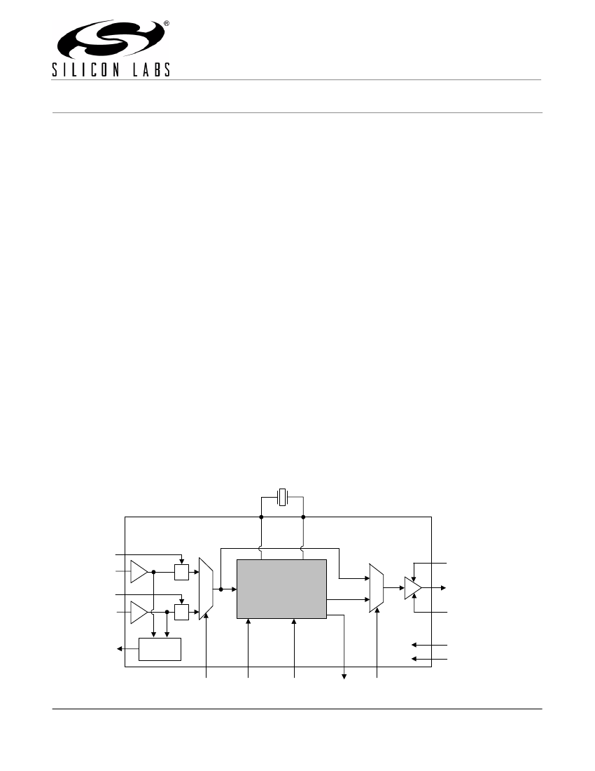
Xtal or Refclock
CK1DIV
CKIN1
CK2DIV
梅
Signal Format
DSPLL
廬
梅
Signal
Detect
CKOUT
Disable
CKIN2
Loss of Signal
VDD (1.8, 2.5, or 3.3 V)
GND
Clock
Select
Frequency Bandwidth
Select
Select
Loss of
Lock
PLL
Bypass
Preliminary Rev. 0.24 3/07
Copyright 漏 2007 by Silicon Laboratories
Si5316
This information applies to a product under development. Its characteristics and specifications are subject to change without notice.


 1
1
 2
2
 3
3
 4
4
 5
5
 6
6
 7
7
 8
8
 9
9
 10
10
 11
11
 12
12
 13
13
 14
14
 15
15
 16
16
