NTE2944
MOSFET
N鈥揅hannel, Enhancement Mode
High Speed Switch
Features:
D
Low Static Drain鈥揝ource ON Resistance
D
Improved Inductive Ruggedness
D
Fast Switching Times
D
Low Input Capacitance
D
Extended Safe Operating Area
D
Improved High Temperature Reliability
D
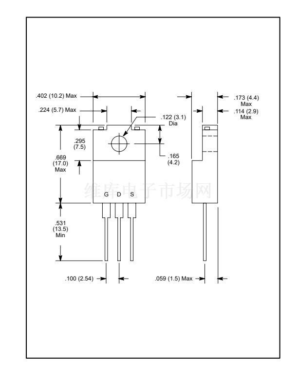
TO220 Type Isolated Package
Absolute Maximum Ratings:
Drain鈥揝ource Voltage (Note 1), V
DSS
. . . . . . . . . . . . . . . . . . . . . . . . . . . . . . . . . . . . . . . . . . . . . . . . 200V
Drain鈥揋ate Voltage (R
GS
= 1M鈩? Note 1), V
DGR
. . . . . . . . . . . . . . . . . . . . . . . . . . . . . . . . . . . . . . 200V
Gate鈥揝ource Voltage, V
GS
. . . . . . . . . . . . . . . . . . . . . . . . . . . . . . . . . . . . . . . . . . . . . . . . . . . . . . . . .
鹵20V
Drain Current, I
D
Continuous
T
C
= +25擄C . . . . . . . . . . . . . . . . . . . . . . . . . . . . . . . . . . . . . . . . . . . . . . . . . . . . . . . . . . . . . . 9.8A
T
C
= +100擄C . . . . . . . . . . . . . . . . . . . . . . . . . . . . . . . . . . . . . . . . . . . . . . . . . . . . . . . . . . . . . 6.8A
Pulsed (Note 2) . . . . . . . . . . . . . . . . . . . . . . . . . . . . . . . . . . . . . . . . . . . . . . . . . . . . . . . . . . . . . . 72A
Gate Current (Pulsed), I
GM
. . . . . . . . . . . . . . . . . . . . . . . . . . . . . . . . . . . . . . . . . . . . . . . . . . . . . . . .
鹵1.5A
Single Pulsed Avalanche Energy (Note 3), E
AS
. . . . . . . . . . . . . . . . . . . . . . . . . . . . . . . . . . . . . . 178mJ
Avalanche Current, I
AS
. . . . . . . . . . . . . . . . . . . . . . . . . . . . . . . . . . . . . . . . . . . . . . . . . . . . . . . . . . . . . 9.8A
Total Power Dissipation (T
C
= +25擄C), P
D
. . . . . . . . . . . . . . . . . . . . . . . . . . . . . . . . . . . . . . . . . . . . 40W
Derate Above 25擄C . . . . . . . . . . . . . . . . . . . . . . . . . . . . . . . . . . . . . . . . . . . . . . . . . . . . . . 0.32W/擄C
Operating Junction Temperature Range, T
J
. . . . . . . . . . . . . . . . . . . . . . . . . . . . . . . . . . 鈥?5擄 to +150擄C
Storage Temperature Range, T
stg
. . . . . . . . . . . . . . . . . . . . . . . . . . . . . . . . . . . . . . . . . . 鈥?5擄 to +150擄C
Maximum Lead Temperature (During Soldering, 1/8鈥?from case, 5sec), T
L
. . . . . . . . . . . . . . +300擄C
Thermal Resistance:
Maximum Junction鈥搕o鈥揅ase, R
thJC
. . . . . . . . . . . . . . . . . . . . . . . . . . . . . . . . . . . . . . . . . 3.12K/W
Typical Case鈥搕o鈥揝ink (Mounting surface flat, smooth, and greased), R
thCS
. . . . . . . 0.5K/W
Maximum Junction鈥搕o鈥揂mbient (Free Air Operation), R
thJA
. . . . . . . . . . . . . . . . . . . . 62.5K/W
Note 1. T
J
= +25擄 to +150擄C.
Note 2. Repetitive Rating: Pulse width limited by maximum junction temperature.
Note 3. L = 2.7mH, V
DD
= 50V, R
G
= 25鈩? Starting T
J
= +25擄C.


 1
1
 2
2
 3
3
