OBJECTIVE PRODUCT SPECIFICATION
10-Bit 125MSPS Sampling
Digital-to-Analog Converter
FEATURES
?
?
?
?
?
?
?
?
1.2V power supply
SFDR > 60dB for (f
in
= 5MHz)
Low power (55mW@1.2V)
Update rate: 125MSPS
Differential output (2 鈥?15mA)
Internal voltage reference
Edge-triggered input latches
Power Down mode
nDA10125-13
APPLICATIONS
?
?
?
?
?
?
Wireless LAN
Basestations
Digital radio link
Set top boxes
Instrumentation
Digital video systems
GENERAL DESCRIPTION
Functional block diagram
The nDA10125-13 is a compact,
0.1
?
F
high-speed, low power 10-bit digital-
Vpbias
AVDD
to-analog converter, implemented in a
PWD
0.13? m pure digital CMOS process.
Vref
The power consumption is only
Vref
55mW from a 1.2V supply operating
Current
Output
Ioutp
0.1
?
F
Bias
at 125MHz update rate. The
Source
Current
Ioutn
Source
Array
Switches
nDA10125-13 offer good AC and DC
R
load
performance at update rates up to
50
?
Iref
125MHz.
R
set
Thermometer Coding/
The DAC has differential current
Latches
outputs with a nominal full-scale
CLK
D[9:0]
output current of 15mA. The full-
scale output range is adjustable
between 2mA and 15mA using the
external R
set
resistor. It operates from
a single 1.2V power supply, and despite this low supply voltage the output compliance
voltage range is as large as 0.5V.
R
load
50
?
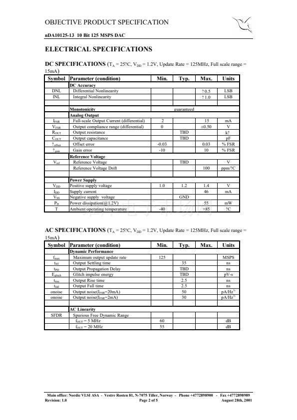
QUICK REFERENCE DATA
Symbol
V
DD
I
DD
P
D
DNL
INL
f
clk,max
SFDR
N
Parameter
Supply Voltage
Supply Current
Power Dissipation
Differential nonlinearity
Integral nonlinearity
Maximum update rate
Spurious free dynamic
range
Resolution
Conditions
125 MSPS
125 MSPS, 1.2V
Min.
1.0
Typ.
1.2
Max.
1.4
46
55
鹵0.5
?
1
Unit
V
mA
mW
LSB
LSB
MHz
dB
bit
125 MSPS,
f
OUT
=5MHz
125
60
10
Main office: Nordic VLSI ASA - Vestre Rosten 81, N-7075 Tiller, Norway - Phone +4772898900 - Fax +4772898989
Revision: 1.0
Page 1 of 5
August 28th, 2001


 1
1
 2
2
 3
3
 4
4
 5
5
