0.235鈩?/div>
I
D
13A
Benefits
l
Low Gate to Drain Charge to Reduce
Switching Losses
l
Fully Characterized Capacitance Including
Effective C
OSS
to Simplify Design, (See
App. Note AN1001)
l
Fully Characterized Avalanche Voltage
and Current
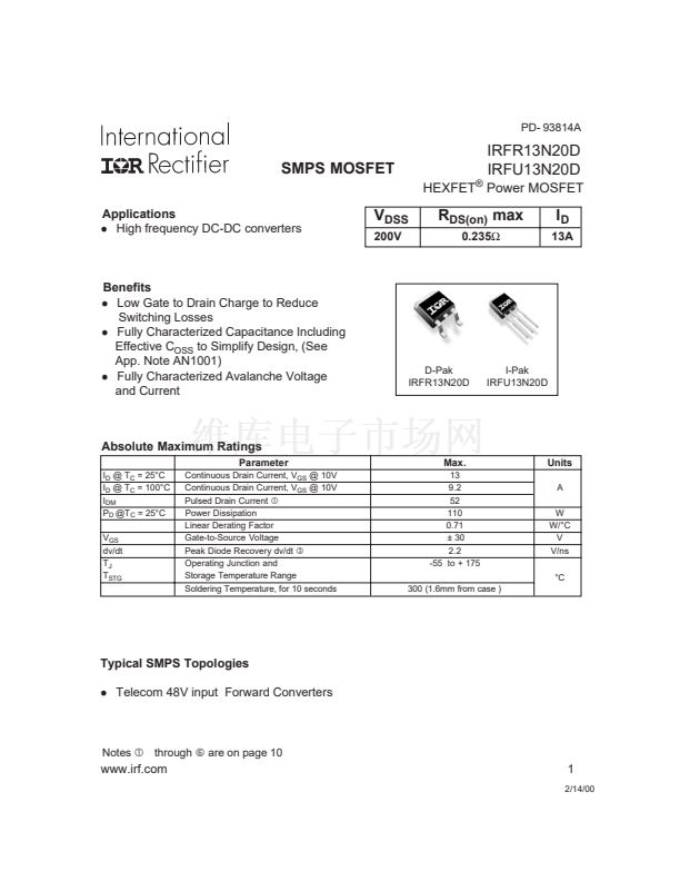
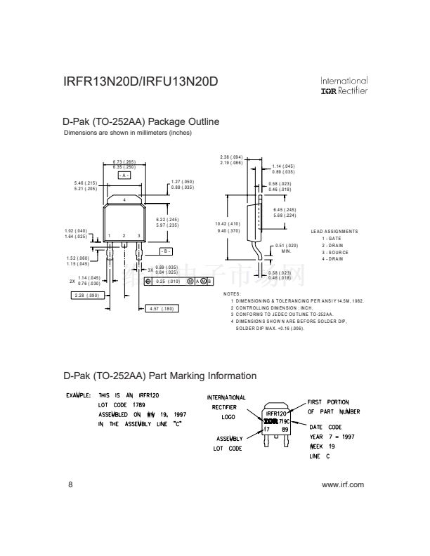
D-Pak
IRFR13N20D
I-Pak
IRFU13N20D
Absolute Maximum Ratings
Parameter
I
D
@ T
C
= 25擄C
I
D
@ T
C
= 100擄C
I
DM
P
D
@T
C
= 25擄C
V
GS
dv/dt
T
J
T
STG
Continuous Drain Current, V
GS
@ 10V
Continuous Drain Current, V
GS
@ 10V
Pulsed Drain Current
聛
Power Dissipation
Linear Derating Factor
Gate-to-Source Voltage
Peak Diode Recovery dv/dt
聝
Operating Junction and
Storage Temperature Range
Soldering Temperature, for 10 seconds
Max.
13
9.2
52
110
0.71
鹵 30
2.2
-55 to + 175
300 (1.6mm from case )
Units
A
W
W/擄C
V
V/ns
擄C
Typical SMPS Topologies
l
Telecom 48V input Forward Converters
Notes
聛
through
聠
are on page 10
www.irf.com
1
2/14/00


 1
1
 2
2
 3
3
 4
4
 5
5
 6
6
 7
7
 8
8
 9
9
 10
10
