typ.
0.28鈩?/div>
T
rr
170ns
I
D
16A
Benefits
Low Gate Charge Qg results in Simple Drive Requirement
Improved Gate, Avalanche and Dynamic dv/dt Ruggedness
Fully Characterized Capacitance and Avalanche Voltage
and Current
Low Trr and Soft Diode Recovery
High Performance Optimised Anti-parallel Diode
Parameter
I
D
@ T
C
= 25擄C
I
D
@ T
C
= 100擄C
I
DM
P
D
@T
C
= 25擄C
V
GS
dv/dt
T
J
T
STG
Continuous Drain Current, V
GS
@ 10V
Continuous Drain Current, V
GS
@ 10V
Pulsed Drain Current
聛
Power Dissipation
Linear Derating Factor
Gate-to-Source Voltage
Peak Diode Recovery dv/dt
聝
Operating Junction and
Storage Temperature Range
Soldering Temperature, for 10 seconds
(1.6mm from case )
Mounting Torque, 6-32 or M3 screw
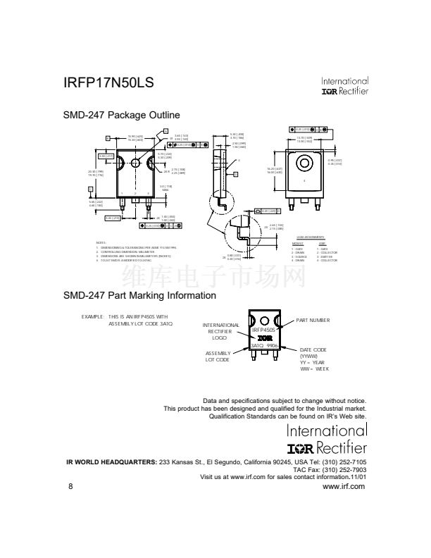
SMD-247
Absolute Maximum Ratings
Max.
16
11
64
220
1.8
鹵 30
13
-55 to + 150
300
10
Units
A
W
W/擄C
V
V/ns
擄C
lbft.in(N.m)
Diode Characteristics
Symbol
I
S
I
SM
V
SD
t
rr
Q
rr
I
RRM
t
on
Parameter
Continuous Source Current
(Body Diode)
Pulsed Source Current
(Body Diode)
聛
Diode Forward Voltage
Reverse Recovery Time
Reverse Recovery Charge
Reverse Recovery Current
Forward Turn-On Time
Min. Typ. Max. Units
Conditions
D
16
MOSFET symbol
鈥撯€撯€?鈥撯€撯€?/div>
showing the
A
G
64
integral reverse
鈥撯€撯€?鈥撯€撯€?/div>
S
p-n junction diode.
鈥撯€撯€?鈥撯€撯€?1.5
V
T
J
= 25擄C, I
S
= 16A, V
GS
= 0V
聞
鈥撯€撯€?170 250
T
J
= 25擄C
I
F
= 16A
ns
鈥撯€撯€?220 330
T
J
= 125擄C
di/dt = 100A/碌s
聞
鈥撯€撯€?470 710
T
J
= 25擄C
nC
鈥撯€撯€?810 1210
T
J
= 125擄C
鈥撯€撯€?7.3
11
A
Intrinsic turn-on time is negligible (turn-on is dominated by L
S
+L
D
)
Typical SMPS Topologies
l
Bridge Converters
l
All Zero Voltage Switching
www.irf.com
1
11/28/01


 1
1
 2
2
 3
3
 4
4
 5
5
 6
6
 7
7
 8
8
