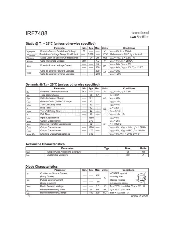
PD - 94507
IRF7488
HEXFET
廬
Power MOSFET
Applications
l
High frequency DC-DC converters
Benefits
l
Low Gate-to-Drain Charge to Reduce
Switching Losses
l
Fully Characterized Capacitance Including
Effective C
OSS
to Simplify Design, (See
App. Note AN1001)
l
Fully Characterized Avalanche Voltage
and Current
V
DSS
80V
R
DS(on)
max
29mW@V
GS
=10V
Q
g
38nC
S
S
S
G
1
8
7
A
A
D
D
D
D
2
3
6
4
5
Top View
SO-8
Absolute Maximum Ratings
Symbol
V
DS
V
GS
I
D
@ T
A
= 25擄C
I
D
@ T
A
= 70擄C
I
DM
P
D
@T
A
= 25擄C
P
D
@T
A
= 70擄C
T
J
T
STG
Parameter
Drain-Source Voltage
Gate-to-Source Voltage
Continuous Drain Current, V
GS
@ 10V
Continuous Drain Current, V
GS
@ 10V
Pulsed Drain Current聛
Maximum Power Dissipation
Maximum Power Dissipation
Linear Derating Factor
Operating Junction and
Storage Temperature Range
Soldering Temperature, for 10 seconds
Max.
80
鹵 20
6.3
5.0
50
2.5
1.6
20
-55 to + 150
300 (1.6mm from case )
Units
V
A
W
mW/擄C
擄C
Thermal Resistance
Symbol
R
胃JL
R
胃JA
Parameter
Junction-to-Drain Lead
Junction-to-Ambient
聞
Typ.
鈥撯€撯€?/div>
鈥撯€撯€?/div>
Max.
20
50
Units
擄C/W
Notes
聛
through
聞
are on page 9
www.irf.com
1
9/23/02


 1
1
 2
2
 3
3
 4
4
 5
5
 6
6
 7
7
 8
8
 9
9
