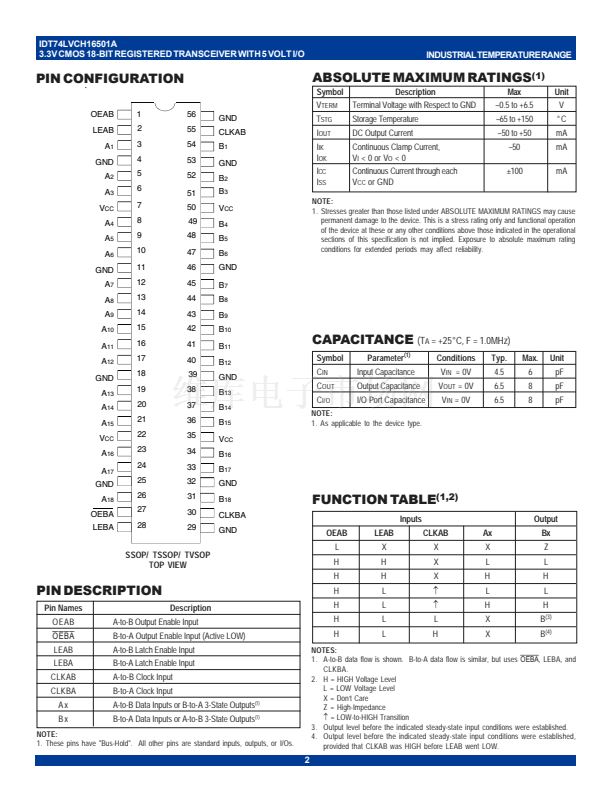
IDT74LVCH16501A
3.3V CMOS 18-BIT REGISTERED TRANSCEIVER WITH 5 VOLT I/O
INDUSTRIAL TEMPERATURE RANGE
3.3V CMOS 18-BIT
IDT74LVCH16501A
REGISTERED BUS TRANSCEIVER
WITH 5V TOLERANT I/O
AND BUS-HOLD
鈥?Typical t
SK(o)
(Output Skew) < 250ps
鈥?ESD > 2000V per MIL-STD-883, Method 3015; > 200V using
machine model (C = 200pF, R = 0)
鈥?V
CC
= 3.3V 鹵 0.3V, Normal Range
鈥?V
CC
= 2.7V to 3.6V, Extended Range
鈥?CMOS power levels (0.4碌 W typ. static)
碌
鈥?All inputs, outputs, and I/O are 5V tolerant
鈥?Supports hot insertion
鈥?Available in SSOP, TSSOP, and TVSOP packages
FEATURES:
DESCRIPTION:
DRIVE FEATURES:
APPLICATIONS:
鈥?High Output Drivers: 鹵24mA
鈥?Reduced system switching noise
鈥?5V and 3.3V mixed voltage systems
鈥?Data communication and telecommunication systems
This 18-bit registered transceiver is built using advanced dual metal
CMOS technology. This high-speed, low power 18-bit registered bus
transceiver combines D-type latches and D-type flip-flops to allow data flow
in transparent latched and clocked modes. Data flow in each direction is
controlled by output-enable (OEAB and
OEBA),
latch enable (LEAB and
LEBA) and clock (CLKAB and CLKBA) inputs. For A-to-B data flow, the
device operates in transparent mode when LEAB is high. When LEAB is
low, the A data is latched if CLKAB is held at a high or low logic level. If LEAB
is low, the A bus data is stored in the latch/flip-flop on the low-to-high transition
of CLKAB. OEAB performs the output enable function on the B port. Data
flow from B port to A port is similar but requires using
OEBA,
LEBA and
CLKBA. Flow-through organization of signal pins simplifies layout. All inputs
are designed with hysteresis for improved noise margin.
The LVCH16501A has been designed with a 鹵24mA output driver. This
driver is capable of driving a moderate to heavy load while maintaining
speed performance.
The LVCH16501A has 鈥渂us-hold鈥?which retains the inputs鈥?last state
whenever the input goes to a high impedance. This prevents floating inputs
and eliminates the need for pull-up/down resistors.
FUNCTIONAL BLOCK DIAGRAM
OEAB
CLKBA
1
30
LEBA
OEBA
CLKAB
LEAB
28
27
55
2
C
3
C
D
54
A
1
D
B
1
C
D
C
D
TO 17 O THER CHANNELS
The IDT logo is a registered trademark of Integrated Device Technology, Inc.
INDUSTRIAL TEMPERATURE RANGE
1
漏 1999 Integrated Device Technology, Inc.
OCTOBER 1999
DSC-3688/1


 1
1
 2
2
 3
3
 4
4
 5
5
 6
6
 7
7
