鈥?/div>
0.5 MICRON CMOS Technology
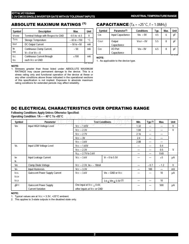
ESD > 2000V per MIL-STD-883, Method 3015;
> 200V using machine model (C = 200pF, R = 0)
0.65mm pitch PSOP package
Industrial temperature range of 鈥?40擄C to +85擄C
V
CC
= 3.3V 鹵0.3V, Normal Range
V
CC
= 1.65V to 3.6V, Extended Range
V
CC
= 2.5V 鹵0.2V
CMOS power levels (0.4碌 W typ. static)
Rail-to-Rail output swing for increased noise margin
All inputs are 5 Volt tolerant
IDT74LVC1GU04A
DESCRIPTION:
This single inverter gate is built using advanced dual metal CMOS
technology. The LVC1GU04A contains one inverter with an unbuffered
output. The device performs the Boolean function Y =
A.
The LVC1GU04A has been designed with a 鹵24mA output driver. This
driver is capable of driving a moderate to heavy load while maintaining
speed performance.
Inputs can be driven from either 3.3V or 5V devices. This feature allows
the use of this device as a translator in a mixed 3.3V/5V supply system.
Drive Features for LVC1GU04A:
鈥?High Output Drivers: 鹵24mA
鈥?Suitable for heavy loads
APPLICATIONS:
鈥?5V and 3.3V mixed voltage systems
鈥?Data communication and telecommunication systems
FUNCTIONAL BLOCK DIAGRAM
PIN CONFIGURATION
1
2 SO5-1
3
4
Y
5
A
2
4
Y
NC
A
GND
V
CC
PSOP
TOP VIEW
PIN DESCRIPTION
Pin Names
A
Y
NC
Description
Data Input
Data Output
No Internal Connection
FUNCTION TABLE
Input
A
H
L
NOTE:
1. H = HIGH Voltage Level
L = LOW Voltage Level
(1)
Output
Y
L
H
INDUSTRIAL TEMPERATURE RANGE
1
c
2000 Integrated Device Technology, Inc.
MAY 2000
DSC-4759/-


 1
1
 2
2
 3
3
 4
4
 5
5
 6
6
