鈥?/div>
Bidirectional interface between GTLP and LVTTL logic levels
Edge Rate Control Circuit reduces output noise
V
REF
pin provides reference voltage for receiver threshold
CMOS technology for low power dissipation
Special PVT Compensation circuitry to provide consistent perfor-
mance over variations of process, supply voltage, and temperature
5V tolerant inputs on LVTTL ports
Bus-Hold to eliminate the need for external pull-up resistors for
unused inputs to A-Port
Power up/down and power-off high-impedance for live insertion
TTL-compatible Driver and Control inputs
High Output source/sink 鹵24mA on A-Port pins
Flow-through architecture optimizes system layout
Open drain on GTLP to support wired OR connection
ESD performance of >2000V
Available in TSSOP package
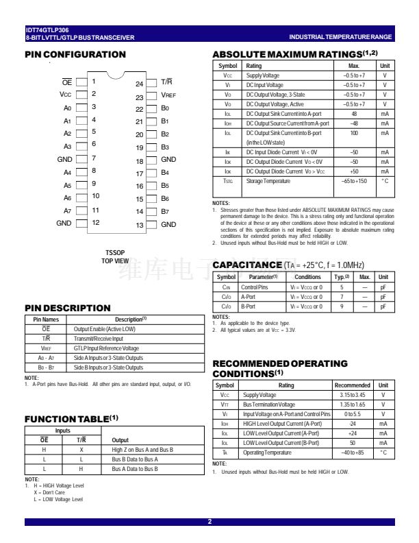
DESCRIPTION:
The GTLP306 is an 8-bit bus transceiver. It provides signal level
translation, from LVTTL to GTLP, for applications requiring a high-speed
interface between cards operating at LVTTL logic levels and back-planes
operating at GTLP logic levels. GTLP provides reduced output swing
(<1V), reduced input threshold levels, and output edge-rate control to
minimize signal setting times. The GTLP306 is a derivative of the Gunning
Transceiver Logic (GTL) JEDEC standard JESD8-3 and incorporates
internal edge-rate control, which is process, voltage, and temperature
(PVT) compensated.
The GTLP306 combines a transceiver function with an LVTTL to GTLP
translation. Data polarity is non-inverting, and the data flow direction is
controlled by the T/R pin. The outputs are enabled to allow data through
the device when
OE
is low. Otherwise, both A and B are placed in a high-
impedance state.
GTLP output low voltage is less than 0.5V. The output high is 1.5V, and
the receiver threshold is 1V.
FUNCTIONAL BLOCK DIAGRAM
T/R
OE
A0 (LVTTL I/O)
B0 (GTLP I/O)
TO SEVEN OTHER CHANNELS
The IDT logo is a registered trademark of Integrated Device Technology, Inc.
INDUSTRIAL TEMPERATURE RANGE
1
c
2002 Integrated Device Technology, Inc.
MAY 2002
DSC-5978/8


 1
1
 2
2
 3
3
 4
4
 5
5
 6
6
 7
7
