鈮?/div>
1碌A (max.)
CMOS power levels
True TTL input and output compatibility:
鈥?V
OH
= 3.3V (typ.)
鈥?V
OL
= 0.3V (typ.)
High Drive outputs (-15mA I
OH
, 48mA I
OL
)
Meets or exceeds JEDEC standard 18 specifications
Military product compliant to MIL-STD-883, Class B and DESC
listed (dual marked)
Power off disable outputs permit "live insertion"
Available in the following packages:
鈥?Industrial: SOIC, SSOP, QSOP
鈥?Military: CERDIP, LCC, CERPACK
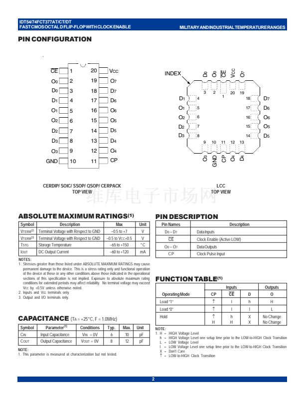
DESCRIPTION:
The IDT54/74FCT377T is an octal D flip-flop built using an advanced
dual metal CMOS technology. The IDT54/74FCT377T has eight edge-
triggered, D-type flip-flops with individual D inputs and O outputs. The
common buffered Clock (CP) input loads all flip-flops simultaneously when
the Clock Enable (CE) is low. The register is fully edge-triggered. The state
of each D input, one set-up time before the low-to-high clock transition, is
transferred to the corresponding flip-flop鈥檚 O output. The
CE
input must be
stable only one set-up time prior to the low-to-high transition for predictable
operation.
FUNCTIONAL BLOCK DIAGRAM
D
0
D
1
D
2
D
3
D
4
D
5
D
6
D
7
CE
D
CP
CP
Q
D
CP
Q
D
CP
Q
D
CP
Q
D
CP
Q
D
CP
Q
D
CP
Q
D
CP
Q
O
0
O
1
O
2
O
3
O
4
O
5
O
6
O
7
The IDT logo is a registered trademark of Integrated Device Technology, Inc.
MILITARY AND INDUSTRIAL TEMPERATURE RANGES
1
MAY 2002
DSC-2630/7
漏 2002 Integrated Device Technology, Inc.


 1
1
 2
2
 3
3
 4
4
 5
5
 6
6
