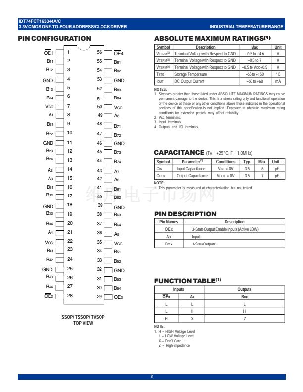
IDT74FCT163344A/C
3.3V CMOS ONE-TO-FOUR ADDRESS/CLOCK DRIVER
INDUSTRIAL TEMPERATURE RANGE
3.3V CMOS ONE-TO-FOUR
ADDRESS/CLOCK DRIVER
IDT74FCT163344A/C
鈥?0.5 MICRON CMOS Technology
鈥?Typical t
SK(o)
(Output Skew) < 250ps
鈥?ESD > 2000V per MIL-STD-883, Method 3015; > 200V using
machine model (C = 200pF, R = 0)
鈥?V
CC
= 3.3V 鹵 0.3V, Normal Range, or V
CC
= 2.7V to 3.6V, Extended
Range
鈥?CMOS power levels (0.4碌 W typ. static)
碌
鈥?Rail-to-rail output swing for increased noise margin
鈥?Low Ground Bounce (0.3V typ.)
鈥?Inputs (except I/O) can be driven by 3.3V or 5V components
鈥?Available in SSOP, TSSOP, and TVSOP packages
FEATURES:
DESCRIPTION:
The FCT163344 is a 1:4 address/clock driver built using advanced dual
metal CMOS technology. This high-speed, low power device provides the
ability to fanout to memory arrays. Eight banks, each with a fanout of 4, and
3-state control provide efficient address distribution. One or more banks may
be used for clock distribution.
The FCT163344 has series current limiting resistors. These offer low
ground bounce, minimal undershoot and controlled output fall times,
reducing the need for external series terminating resistors.
A large number of power and ground pins ensure reduced noise levels.
All inputs are designed with hysteresis for improved noise margins.
The inputs of the FCT163344 can be driven from either 3.3V or 5V device.
This feature allows the use of these devices as translators in a mixed 3.3V/
5V supply system.
FUNCTIONAL BLOCK DIAGRAM
OE
1
1
2
OE
3
B
11
A
5
6
36
29
34
B
51
A
1
8
B
14
B
21
A
6
42
30
B
54
B
61
9
41
A
2
14
13
B
24
37
B
64
OE
2
28
16
OE
4
B
31
A
7
20
43
56
48
B
71
A
3
15
B
34
B
41
A
8
49
44
B
74
B
81
23
55
A
4
21
27
51
B
44
B
84
The IDT logo is a registered trademark of Integrated Device Technology, Inc.
INDUSTRIAL TEMPERATURE RANGE
1
漏 2002 Integrated Device Technology, Inc.
APRIL 2002
DSC-3249/1


 1
1
 2
2
 3
3
 4
4
 5
5
 6
6
 7
7
