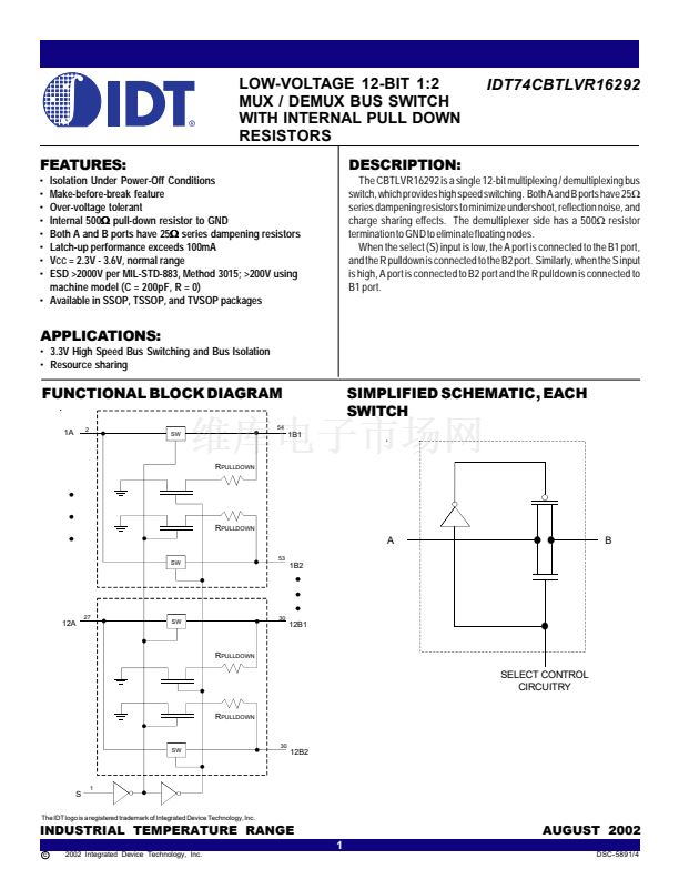
switch, which provides high speed switching. Both A and B ports have 25鈩?/div>
series dampening resistors to minimize undershoot, reflection noise, and
charge sharing effects. The demultiplexer side has a 500鈩?resistor
termination to GND to eliminate floating nodes.
When the select (S) input is low, the A port is connected to the B1 port,
and the R pulldown is connected to the B2 port. Similarly, when the S input
is high, A port is connected to B2 port and the R pulldown is connected to
B1 port.
APPLICATIONS:
鈥?3.3V High Speed Bus Switching and Bus Isolation
鈥?Resource sharing
FUNCTIONAL BLOCK DIAGRAM
1A
2
54
SW
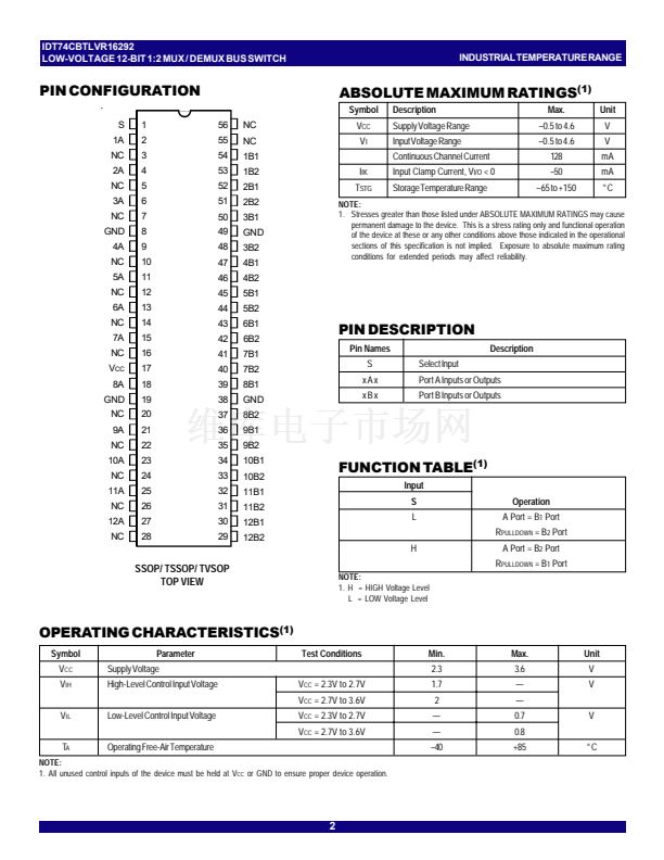
SIMPLIFIED SCHEMATIC, EACH
SWITCH
1B1
R
PULLDOWN
R
PULLDOWN
A
SW
53
B
1B2
12A
27
SW
30
12B1
R
PULLDOWN
SELECT CONTROL
CIRCUITRY
R
PULLDOWN
SW
30
12B2
S
1
INDUSTRIAL TEMPERATURE RANGE
1
c
2002 Integrated Device Technology, Inc.
The IDT logo is a registered trademark of Integrated Device Technology, Inc.
AUGUST 2002
DSC-5891/4


 1
1
 2
2
 3
3
 4
4
 5
5
