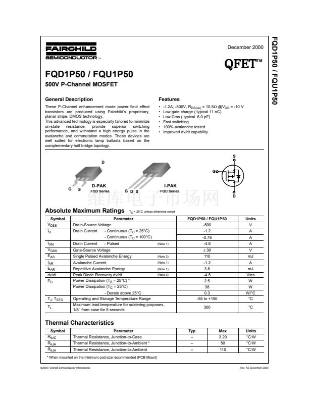
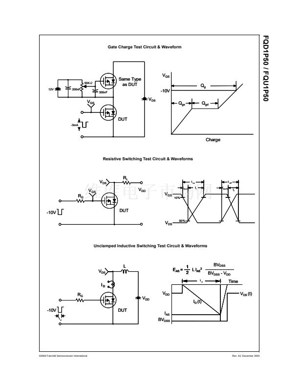
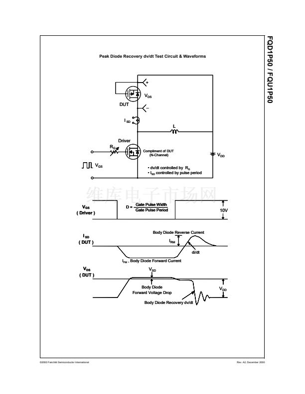
鈼?/div>
G
S
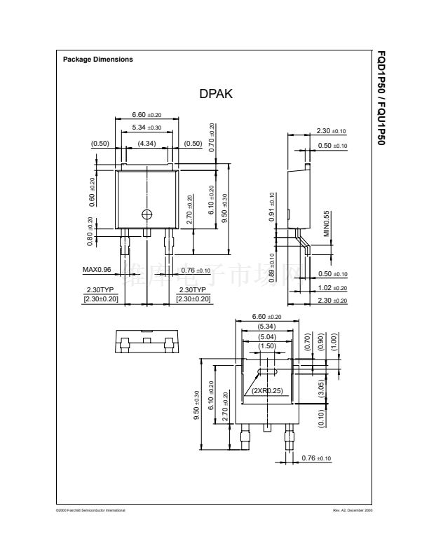
D-PAK
FQD Series
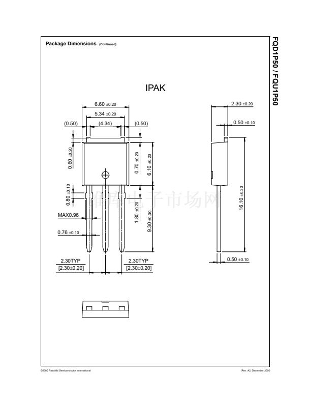
I-PAK
G D S
FQU Series
!
D
Absolute Maximum Ratings
Symbol
V
DSS
I
D
I
DM
V
GSS
E
AS
I
AR
E
AR
dv/dt
P
D
T
C
= 25擄C unless otherwise noted
Parameter
Drain-Source Voltage
- Continuous (T
C
= 25擄C)
Drain Current
- Continuous (T
C
= 100擄C)
Drain Current
- Pulsed
(Note 1)
FQD1P50 / FQU1P50
-500
-1.2
-0.76
-4.8
鹵
30
(Note 2)
(Note 1)
(Note 1)
(Note 3)
Units
V
A
A
A
V
mJ
A
mJ
V/ns
W
W
W/擄C
擄C
擄C
Gate-Source Voltage
Single Pulsed Avalanche Energy
Avalanche Current
Repetitive Avalanche Energy
Peak Diode Recovery dv/dt
Power Dissipation (T
A
= 25擄C) *
Power Dissipation (T
C
= 25擄C)
110
-1.2
3.8
-4.5
2.5
38
0.3
-55 to +150
300
T
J
, T
STG
T
L
- Derate above 25擄C
Operating and Storage Temperature Range
Maximum lead temperature for soldering purposes,
1/8鈥?from case for 5 seconds
Thermal Characteristics
Symbol
R
胃JC
R
胃JA
R
胃JA
Parameter
Thermal Resistance, Junction-to-Case
Thermal Resistance, Junction-to-Ambient *
Thermal Resistance, Junction-to-Ambient
Typ
--
--
--
Max
3.29
50
110
Units
擄C/W
擄C/W
擄C/W
* When mounted on the minimum pad size recommended (PCB Mount)
漏2000 Fairchild Semiconductor International
Rev. A2, December 2000


 1
1
 2
2
 3
3
 4
4
 5
5
 6
6
 7
7
 8
8
 9
9
