鈭?/div>
DS1845-100 one 10k, 100 position &
one 100k, 256 position
256 bytes of EEPROM memory
Access to data and potentiometer control via
a 2-wire interface
External Write Enable pin to protect data and
potentiometer settings
Nonvolatile wiper storage in 2 bytes of
address space
Operates from 3V or 5V supplies
Packaging: Flip Chip Package, 16-ball
STPBGA, 14-pin TSSOP
Industrial operating temperature: -40潞C to
+85潞C
Programming temperature: 0潞C to +70潞C
PIN ASSIGNMENT
SDA
SCL
A0
A1
A2
WP
GND
1
2
3
4
5
6
7
14
13
12
11
10
9
8
Vcc
H0
W1
H1
L1
W0
L0
14-Pin TSSOP (173 mil)
14-Pin Flip Chip (100 x 100 mils)
16-BALL STPBGA (4 x 4 mm)
See Mech. Drawing Section
PIN DESCRIPTION
V
CC
GND
SDA
SCL
WP
A0, A1, A2
H0, H1
L 0, L1
W0, W1
- 3V or 5V Power Supply Input
- Ground
- 2-wire Serial Data
Input/Output
- 2-wire Serial Clock Input
- Write Protect Input
- Address Inputs
- High-End of Potentiometer
- Low-End of Potentiometer
- Wiper Terminal of
Potentiometer
DESCRIPTION
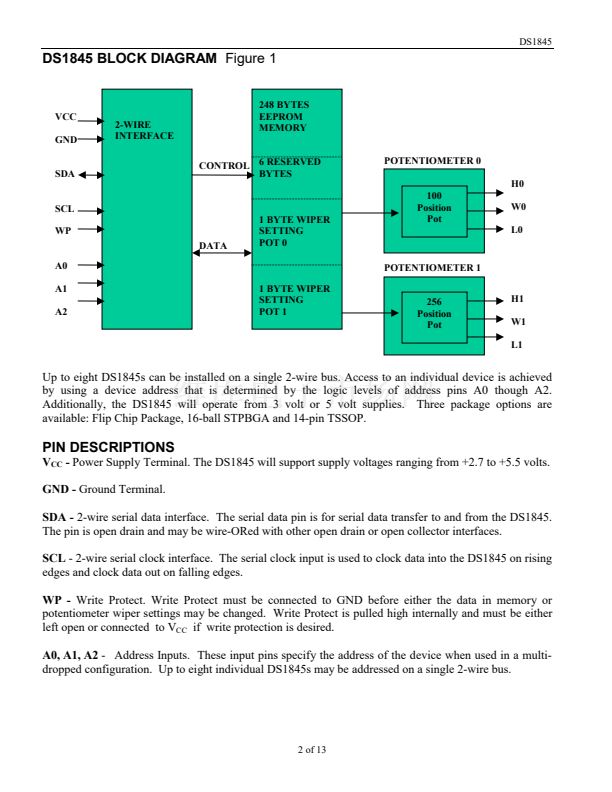
The DS1845 Dual NV Potentiometer and Memory consists of one=100-position linear taper
potentiometer, one=256-position linear taper potentiometer, 256 bytes of EEPROM memory, and a 2-wire
interface. The device provides an ideal method for setting bias voltages and currents in control
applications using a minimum of circuitry. The EEPROM memory allows a user to store configuration
or calibration data for a specific system or device as well as provide control of the potentiometer wiper
settings. Any type of user information may reside in the first 248 bytes of this memory. The next two
addresses of EEPROM memory are for potentiometer settings and the remaining 6 bytes of memory are
reserved. These reserved and potentiometer registers should not be used for data storage. Access to this
EEPROM is via an industry standard 2-wire bus. The interface I/O pins consist of SDA and SCL. The
wiper position of the DS1845, as well as EEPROM data, can be hardware write-protected using the Write
Protect (WP) input pin.
1 of 13
051900


 1
1
 2
2
 3
3
 4
4
 5
5
 6
6
 7
7
 8
8
 9
9
 10
10
 11
11
 12
12
 13
13
