錚?/div>
16-Mbit (2048K x 8) Static RAM
Features
鈥?Very high speed: 55 ns and 70 ns
鈥?Wide voltage range: 2.20V 鈥?3.60V
鈥?Ultra-low active power
鈥?Typical active current: 2 mA @ f = 1 MHz
鈥?Typical active current: 15 mA @ f = f
max
鈥?Ultra-low standby power
鈥?Easy memory expansion with CE
1
, CE
2
and OE features
鈥?Automatic power-down when deselected
鈥?CMOS for optimum speed/power
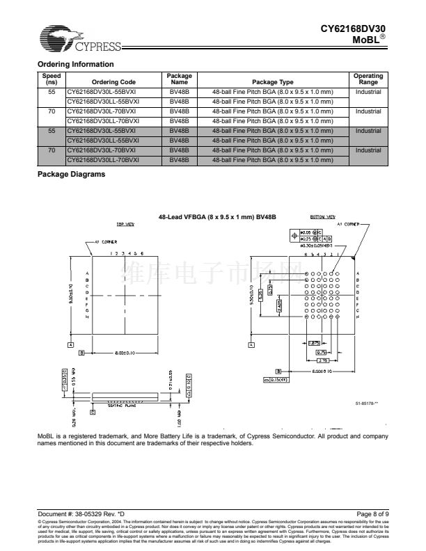
鈥?Packages offered in a 48-ball FBGA
addresses are not toggling. The device can be put into standby
mode reducing power consumption by more than 99% when
deselected Chip Enable 1 (CE
1
) HIGH or Chip Enable 2 (CE
2
)
LOW. The input/output pins (I/O
0
through I/O
7
) are placed in
a high-impedance state when: deselected Chip Enable 1
(CE
1
) HIGH or Chip Enable 2 (CE
2
) LOW, outputs are disabled
(OE HIGH), or during a write operation (Chip Enable 1 (CE
1
)
LOW and Chip Enable 2 (CE
2
) HIGH and WE LOW).
Writing to the device is accomplished by taking Chip Enable 1
(CE
1
) LOW and Chip Enable 2 (CE
2
) HIGH and Write Enable
(WE) input LOW. Data on the eight I/O pins (I/O
0
through I/O
7
)
is then written into the location specified on the address
pins(A
0
through A
20
).
Reading from the device is accomplished by taking Chip
Enable 1 (CE
1
) and Output Enable (OE) LOW and Chip
Enable 2 (CE
2
) HIGH while forcing Write Enable (WE) HIGH.
Under these conditions, the contents of the memory location
specified by the address pins will appear on the I/O pins.
The eight input/output pins (I/O
0
through I/O
7
) are placed in a
high-impedance state when the device is deselected (CE
1
LOW and CE
2
HIGH), the outputs are disabled (OE HIGH), or
during a write operation (CE
1
LOW and CE
2
HIGH and WE
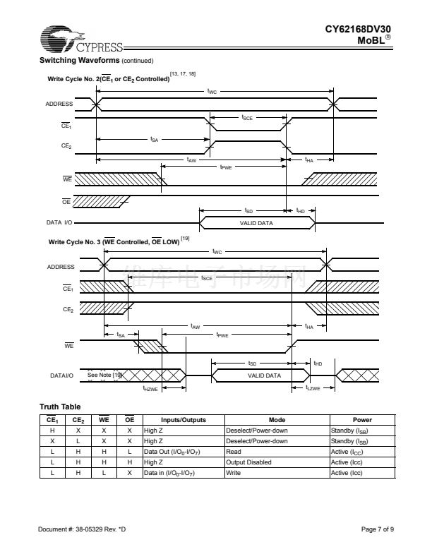
LOW). See the truth table for a complete description of read
and write modes.
Functional Description
[1]
The CY62168DV30 is a high-performance CMOS static RAMs
organized as 2048Kbit words by 8 bits. This device features
advanced circuit design to provide ultra-low active current.
This is ideal for providing More Battery Life錚?(MoBL
錚?/div>
) in
portable applications such as cellular telephones. The device
also has an automatic power-down feature that significantly
reduces power consumption. The device can be put into
standby mode reducing power consumption by 90% when
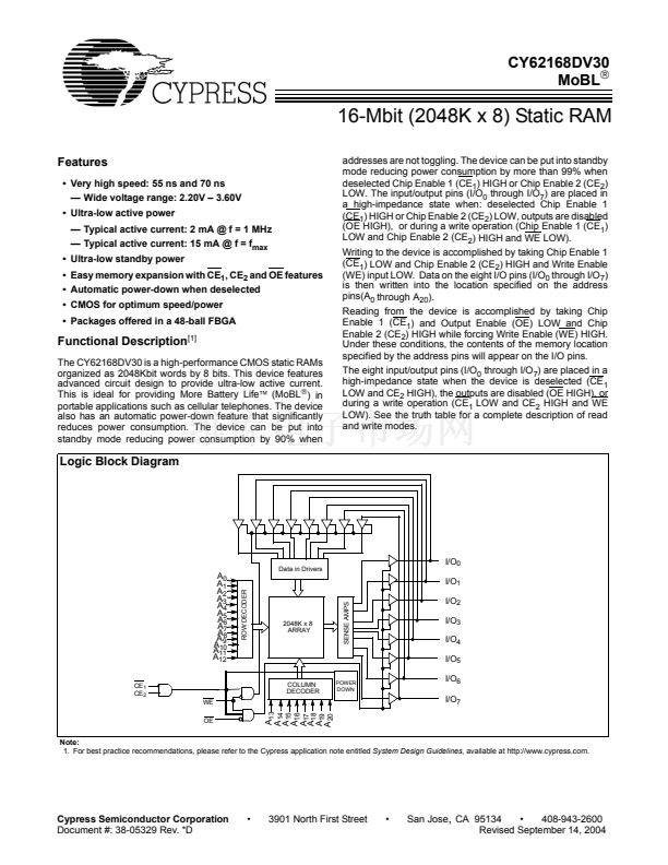
Logic Block Diagram
A
0
A
1
A
2
A
3
A
4
A
5
A
6
A
7
A
8
A
9
A
10
A
11
A
12
CE
1
CE
2
WE
OE
Data in Drivers
I/O
0
I/O
1
ROW DECODER
SENSE AMPS
I/O
2
I/O
3
I/O
4
I/O
5
2048K x 8
ARRAY
COLUMN
DECODER
POWER
DOWN
I/O
6
I/O
7
Note:
1. For best practice recommendations, please refer to the Cypress application note entitled
System Design Guidelines,
available at http://www.cypress.com.
A
17
A
18
A
19
A
20
A
16
A
13
A
14
A
15
Cypress Semiconductor Corporation
Document #: 38-05329 Rev. *D
鈥?/div>
3901 North First Street
鈥?/div>
San Jose
,
CA 95134
鈥?/div>
408-943-2600
Revised September 14, 2004


 1
1
 2
2
 3
3
 4
4
 5
5
 6
6
 7
7
 8
8
 9
9
