鈥?/div>
28
碌W
(max.)
Easy memory expansion with CE and OE features
TTL-compatible inputs and outputs
Automatic power-down when deselected
CMOS for optimum speed/power
Package available in a standard 450-mil-wide (300-mil
body width) 28-lead narrow SOIC, 28-lead TSOP-1,
28-lead reverse TSOP-1, and 600-mil 28-lead PDIP
packages
Functional Description
[1]
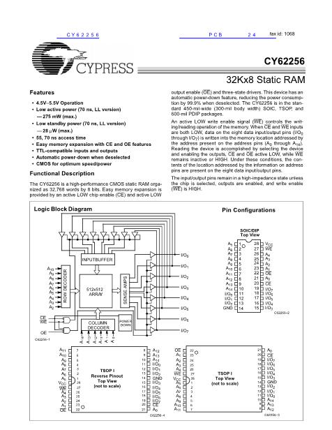
The CY62256 is a high-performance CMOS static RAM
organized as 32K words by 8 bits. Easy memory expansion is
provided by an active LOW chip enable (CE) and active LOW
output enable (OE) and three-state drivers. This device has an
automatic power-down feature, reducing the power
consumption by 99.9% when deselected.
An active LOW write enable signal (WE) controls the
writing/reading operation of the memory. When CE and WE
inputs are both LOW, data on the eight data input/output pins
(I/O
0
through I/O
7
) is written into the memory location
addressed by the address present on the address pins (A
0
through A
14
). Reading the device is accomplished by selecting
the device and enabling the outputs, CE and OE active LOW,
while WE remains inactive or HIGH. Under these conditions,
the contents of the location addressed by the information on
address pins are present on the eight data input/output pins.
The input/output pins remain in a high-impedance state unless
the chip is selected, outputs are enabled, and write enable
(WE) is HIGH.
Logic Block Diagram
INPUTBUFFER
A
10
A
9
A
8
A
7
A
6
A
5
A
4
A
3
A
2
CE
WE
OE
A
14
A
13
A
12
A
11
A
1
A
0
ROW DECODER
I/O
0
I/O
1
SENSE AMPS
I/O
2
I/O
3
I/O
4
I/O
5
512 x 512
Y
ARRA
COLUMN
DECODER
POWER
DOWN
I/O
6
I/O
7
Note:
1. For best practice recommendations, please refer to the Cypress application note 鈥淪ystem Design Guidelines鈥?on http://www.cypress.com.
Cypress Semiconductor Corporation
Document #: 38-05248 Rev. *C
鈥?/div>
3901 North First Street
鈥?/div>
San Jose
鈥?/div>
CA 95134 鈥?408-943-2600
Revised June 25, 2004


 1
1
 2
2
 3
3
 4
4
 5
5
 6
6
 7
7
 8
8
 9
9
 10
10
 11
11
 12
12
