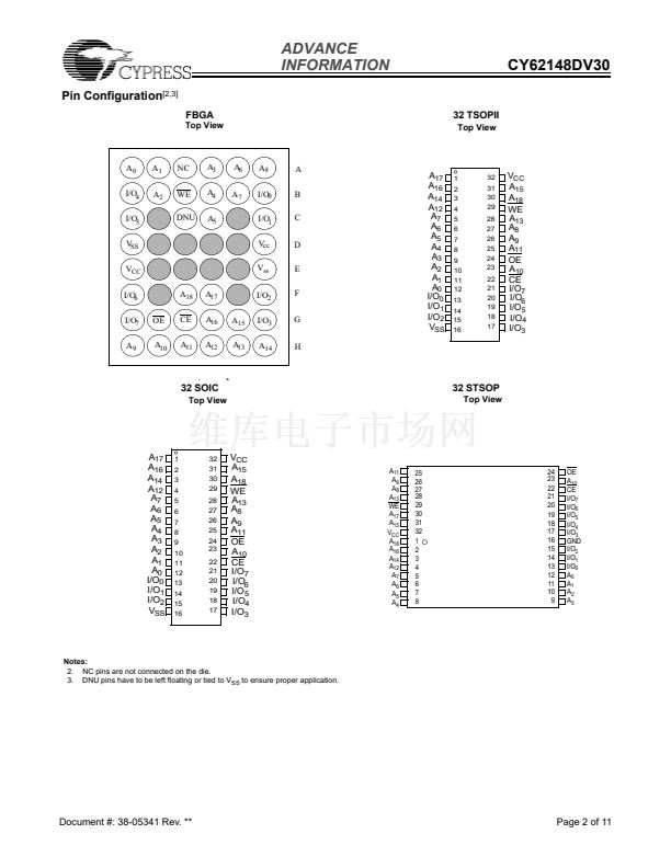
錚?/div>
) in
portable applications such as cellular telephones. The device
also has an automatic power-down feature that significantly
reduces power consumption by 99% when addresses are not
toggling. The device can be put into standby mode reducing
power consumption by more than 99% when deselected (CE
HIGH).
Writing to the device is accomplished by taking Chip Enable
(CE) and Write Enable (WE) inputs LOW. Data on the eight I/O
pins (I/O
0
through I/O
7
) is then written into the location
specified on the address pins (A
0
through A
18
).
Reading from the device is accomplished by taking Chip
Enable (CE) and Output Enable (OE) LOW while forcing Write
Enable (WE) HIGH. Under these conditions, the contents of
the memory location specified by the address pins will appear
on the I/O pins.
The eight input/output pins (I/O
0
through I/O
7
) are placed in a
high-impedance state when the device is deselected (CE
HIGH), the outputs are disabled (OE HIGH), or during a write
operation (CE LOW and WE LOW).
Functional
Description
[1]
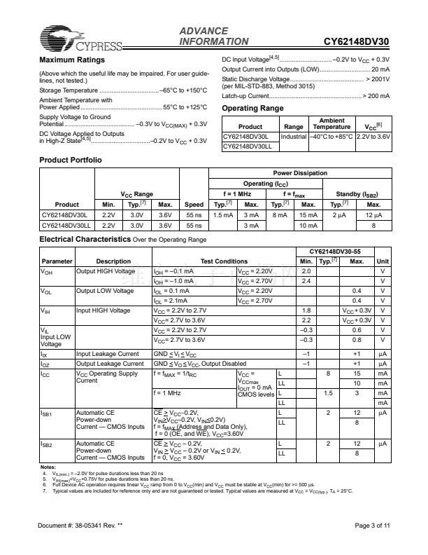
The CY62148DV30 is a high-performance CMOS static RAMs
organized as 512K words by 8 bits. This device features
advanced circuit design to provide ultra-low active current.
Logic Block Diagram
Data in Drivers
I/O
0
I/O
1
A
0
A
1
A
2
A
3
A
4
A
5
A
6
A
7
A
8
A
9
A
10
A
11
A
12
ROW DECODER
SENSE AMPS
I/O
2
I/O
3
I/O
4
I/O
5
512K x 8
ARRAY
CE
WE
OE
COLUMN
DECODER
POWER
DOWN
I/O
6
I/O
7
Note:
1. For best practice recommendations, please refer to the Cypress application note 鈥淪ystem Design Guidelines鈥?on http://www.cypress.com.
A
13
A
14
A
15
A
16
A
17
A
18
Cypress Semiconductor Corporation
Document #: 38-05341 Rev. **
鈥?/div>
3901 North First Street
鈥?/div>
San Jose
,
CA 95134
鈥?/div>
408-943-2600
Revised June 11, 2003


 1
1
 2
2
 3
3
 4
4
 5
5
 6
6
 7
7
 8
8
 9
9
 10
10
 11
11
