鈥?/div>
CY62137CV18: 1.65V鈭?.95V
鈥?Pin Compatible w/ CY62137V18/BV18
鈥?Ultra-low active power
鈥?Typical Active Current: 0.5 mA @ f = 1 MHz
鈥?Typical Active Current: 1.5 mA @ f = f
max
(70 ns
speed)
Low standby power
Easy memory expansion with CE and OE features
Automatic power-down when deselected
CMOS for optimum speed/power
power consumption by 99% when addresses are not toggling.
The device can also be put into standby mode when deselect-
ed (CE HIGH or both BLE and BHE are HIGH). The input/out-
put pins (I/O
0
through I/O
15
) are placed in a high-impedance
state when: deselected (CE HIGH), outputs are disabled (OE
HIGH), both Byte High Enable and Byte Low Enable are dis-
abled (BHE, BLE HIGH), or during a write operation (CE LOW,
and WE LOW).
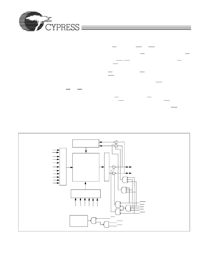
Writing to the device is accomplished by taking Chip Enable
(CE) and Write Enable (WE) inputs LOW. If Byte Low Enable
(BLE) is LOW, then data from I/O pins (I/O
0
through I/O
7
), is
written into the location specified on the address pins (A
0
through A
16
). If Byte High Enable (BHE) is LOW, then data
from I/O pins (I/O
8
through I/O
15
) is written into the location
specified on the address pins (A
0
through A
16
).
Reading from the device is accomplished by taking Chip En-
able (CE) and Output Enable (OE) LOW while forcing the Write
Enable (WE) HIGH. If Byte Low Enable (BLE) is LOW, then
data from the memory location specified by the address pins
will appear on I/O
0
to I/O
7
. If Byte High Enable (BHE) is LOW,
then data from memory will appear on I/O
8
to I/O
15
. See the
Truth Table at the back of this data sheet for a complete de-
scription of read and write modes.
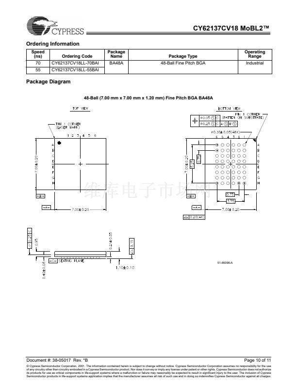
The CY62137CV18 is available in a 48-ball FBGA package.
鈥?/div>
鈥?/div>
鈥?/div>
鈥?/div>
Functional Description
The CY62137CV18 is a high-performance CMOS static RAM
organized as 128K words by 16 bits. This device features ad-
vanced circuit design to provide ultra-low active current. This
is ideal for providing More Battery Life鈩?(MoBL鈩? in portable
applications such as cellular telephones. The device also has
an automatic power-down feature that significantly reduces
Logic Block Diagram
DATA IN DRIVERS
A
10
A
9
ROW DECODER
SENSE AMPS
A
8
A
7
A
6
A
5
A
4
A
3
A
2
A
1
A
0
128K x 16
RAM Array
2048 X 1024
I/O
0
鈥揑/O
7
I/O
8
鈥揑/O
15
COLUMN DECODER
BHE
WE
CE
OE
BLE
CE
BHE
BLE
A
11
A
12
A
13
A
14
A
15
Power -Down
Circuit
MoBL, MoBL2, and More Battery Life are trademarks of Cypress Semiconductor Corporation.
Cypress Semiconductor Corporation
Document #: 38-05017 Rev. *B
鈥?/div>
3901 North First Street
A
16
鈥?/div>
San Jose
鈥?/div>
CA 95134 鈥?408-943-2600
Revised October 31, 2001
CY62137CV18相關(guān)型號PDF文件下載
-
型號
版本
描述
廠商
下載
-
英文版
8K x 8 Static RAM
Cypress
-
英文版
128K x 8 Static RAM
CYPRESS
-
英文版
128K x 8 Static RAM
CYPRESS [C...
-
英文版
512K x 8 MoBL Static RAM
CYPRESS
-
英文版
512K x 8 MoBL Static RAM
CYPRESS [C...
-
英文版
32Kx8 Static RAM
Cypress
-
英文版
64K x 16 Static RAM
Cypress
-
英文版
64K x 16 Static RAM
Cypress
-
英文版
128K x 8 Static RAM
CYPRESS
-
英文版
128K x 8 Static RAM
CYPRESS [C...
-
英文版
1-Mbit (128K x 8) Static RAM
CYPRESS [C...
-
英文版
128K x 8 Static RAM
CYPRESS
-
英文版
128K x 8 Static RAM
CYPRESS [C...
-
英文版
128K x 16 Flash Compatible Static RAM
Cypress
-
英文版
Memory
ETC
-
英文版
128K x 16 Static RAM
Cypress
-
英文版
2-Mbit (128K x 16) Static RAM
CYPRESS
-
英文版
2-Mbit (128K x 16) Static RAM
CYPRESS [C...
-
英文版
Cypress Semiconductor [2-Mbit (256K x 8) Static RAM]
CYPRESS
-
英文版
256K x 8 Static RAM
CYPRESS


 1
1
 2
2
 3
3
 4
4
 5
5
 6
6
 7
7
 8
8
 9
9
 10
10
 11
11
