CD74FCT240AT and CD74FCT244AT were not acquired from Harris Semiconductor.
Data sheet acquired from Harris Semiconductor
SCHS270A
CD54/74FCT240, CD54/74FCT240AT,
CD54/74FCT241, CD54/74FCT244,
CD54/74FCT244AT
FCT Interface Logic
Octal Buffers/Line Drivers, Three-State
Description
The CD54/74FCT240, 240AT, 241, 244 and 244AT three-
state octal buffers/line drivers use a small-geometry
BiCMOS technology. The output stage is a combination of
bipolar and CMOS transistors that limits the output-HIGH
level to two diode drops below VCC. This resultant lowering
of output swing (0V to 3.7V) reduces power bus ringing (a
source of EMI) and minimizes VCC bounce and ground
bounce and their effects during simultaneous output
switching. The output con鏗乬uration also enhances switching
speed and is capable of sinking 48mA to 64mA.
The CD54/74FCT240, 240AT, 244 and 244AT have active-
LOW output enables (1OE, 2OE). The CD54/74FCT241 and
CD54/74FCT241AT have one active-LOW (1OE) and one
active-HIGH (2OE) output enable.
February 1996
Features
鈥?CD54/74FCT240, CD54/74FCT240AT - Inverting
鈥?CD54/74FCT241, CD54/74FCT244, CD54/74FCT244AT -
Non-Inverting
鈥?Buffered Inputs
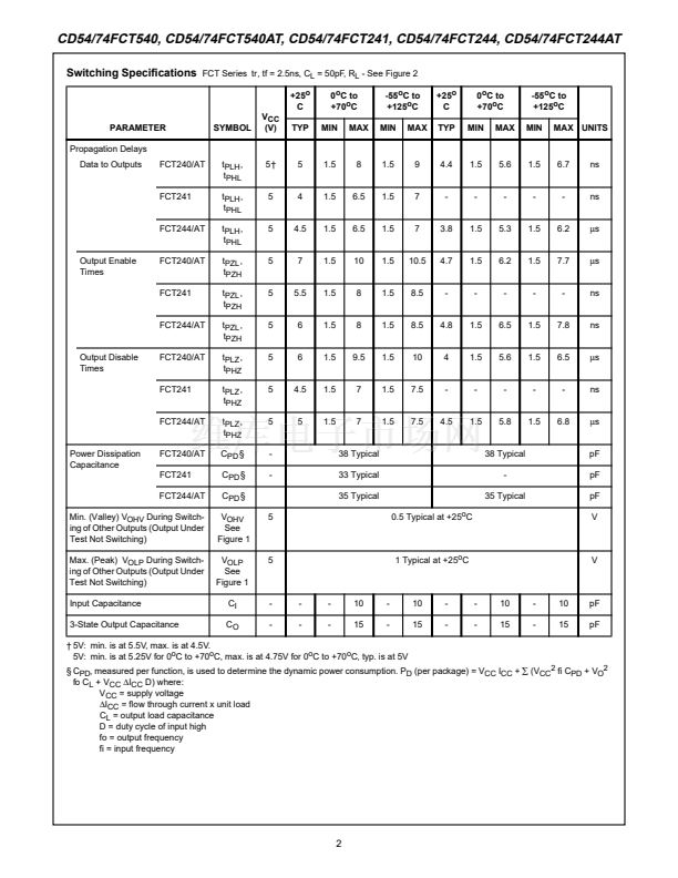
鈥?Typical Propagation Delay:
4.1ns at VCC = 5V, TA = 25
o
C (FCT240AT, FCT244AT)
鈥?SCR-Latchup-Resistant BiCMOS Process and Circuit
Design
鈥?FCTXXX Types - Speed of Bipolar FAST
廬
/AS/S;
FCTXXXAT Types - 30% Faster Than FAST/AS/S with
Signi鏗乧antly Reduced Power Consumption
鈥?48mA to 64mA Output Sink Current (Commer-
cial/Extended Industrial)
鈥?Output Voltage Swing Limited to 3.7V at VCC = 5V
鈥?Controlled Output-Edge Rates
鈥?Input/Output Isolation to VCC
鈥?BiCMOS Technology with Low Quiescent Power
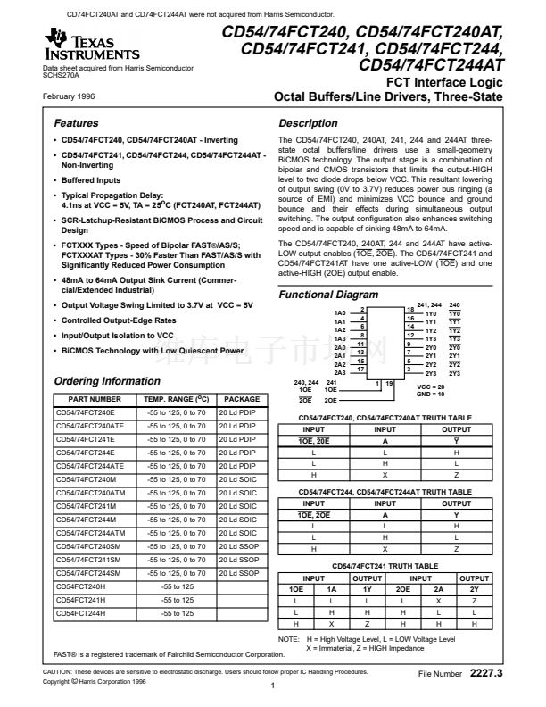
Functional Diagram
1A0
1A1
1A2
1A3
2A0
2A1
2A2
2A3
240, 244 241
1OE
1OE
2OE
2OE
2
4
6
8
11
13
15
17
1
19
18
16
14
12
9
7
5
3
241, 244
1Y0
1Y1
1Y2
1Y3
2Y0
2Y1
2Y2
2Y3
VCC = 20
GND = 10
240
1Y0
1Y1
1Y2
1Y3
2Y0
2Y1
2Y2
2Y3
Ordering Information
PART NUMBER
CD54/74FCT240E
CD54/74FCT240ATE
CD54/74FCT241E
CD54/74FCT244E
CD54/74FCT244ATE
CD54/74FCT240M
CD54/74FCT240ATM
CD54/74FCT241M
CD54/74FCT244M
CD54/74FCT244ATM
CD54/74FCT240SM
CD54/74FCT241SM
CD54/74FCT244SM
CD54FCT240H
CD54FCT241H
CD54FCT244H
TEMP. RANGE (
o
C)
-55 to 125, 0 to 70
-55 to 125, 0 to 70
-55 to 125, 0 to 70
-55 to 125, 0 to 70
-55 to 125, 0 to 70
-55 to 125, 0 to 70
-55 to 125, 0 to 70
-55 to 125, 0 to 70
-55 to 125, 0 to 70
-55 to 125, 0 to 70
-55 to 125, 0 to 70
-55 to 125, 0 to 70
-55 to 125, 0 to 70
-55 to 125
-55 to 125
-55 to 125
PACKAGE
20 Ld PDIP
20 Ld PDIP
20 Ld PDIP
20 Ld PDIP
20 Ld PDIP
20 Ld SOIC
20 Ld SOIC
20 Ld SOIC
20 Ld SOIC
20 Ld SOIC
20 Ld SSOP
20 Ld SSOP
20 Ld SSOP
CD54/74FCT240, CD54/74FCT240AT TRUTH TABLE
INPUT
1OE, 20E
L
L
H
INPUT
A
L
H
X
OUTPUT
Y
H
L
Z
CD54/74FCT244, CD54/74FCT244AT TRUTH TABLE
INPUT
1OE, 2OE
L
L
H
INPUT
A
L
H
X
CD54/74FCT241 TRUTH TABLE
INPUT
1OE
L
L
H
NOTE:
1A
L
H
X
OUTPUT
1Y
L
H
Z
L
H
H
INPUT
2OE
2A
X
L
H
OUTPUT
2Y
Z
L
H
OUTPUT
Y
H
L
Z
H = High Voltage Level, L = LOW Voltage Level
X = Immaterial, Z = HIGH Impedance
FAST廬 is a registered trademark of Fairchild Semiconductor Corporation.
CAUTION: These devices are sensitive to electrostatic discharge. Users should follow proper IC Handling Procedures.
Copyright
漏
Harris Corporation 1996
File Number
2227.3
1


 1
1
 2
2
 3
3
