54FCT 74FCT273 Octal D Flip-Flop
March 1993
54FCT 74FCT273
Octal D Flip-Flop
General Description
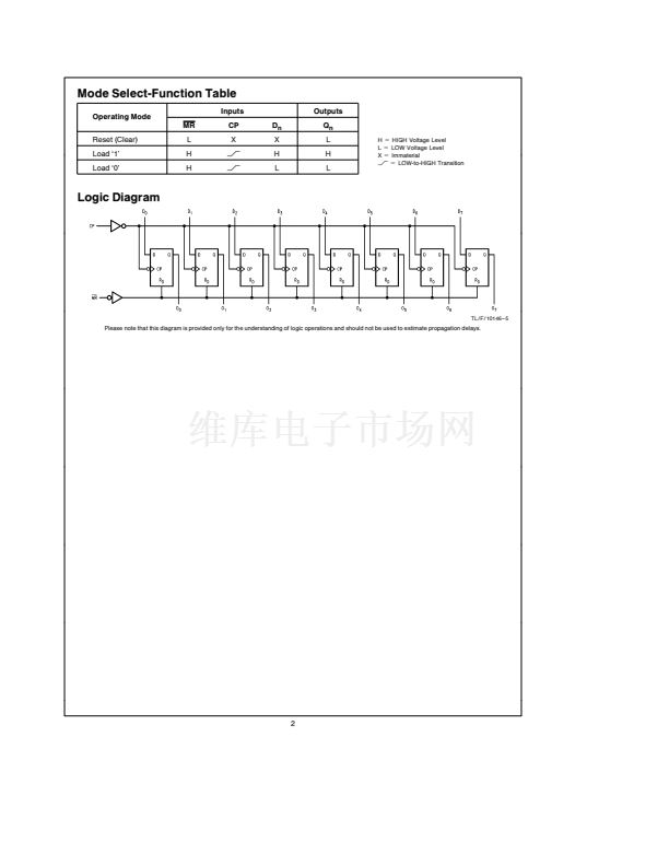
The 鈥橣CT273 has eight edge-triggered D-type flip-flops with
individual D inputs and Q outputs The common buffered
Clock (CP) and Master Reset (MR) input load and reset
(clear) all flip-flops simultaneously
The register is fully edge-triggered The state of each D in-
put one setup time before the LOW-to-HIGH clock tran-
sition is transferred to the corresponding flip-flop鈥檚 Q out-
put
All outputs will be forced LOW independently of Clock or
Data inputs by a LOW voltage level on the MR input The
device is useful for applications where the true output only is
required and the Clock and Master Reset are common to all
storage elements
Features
Y
Y
Y
Y
Y
Y
Y
Y
Y
Y
I
CC
reduced to 40 0
mA
Ideal buffer for MOS microprocessor or memory
Eight edge-triggered D flip-flops
Buffered common clock
Buffered asynchronous master reset
TTL input and output level compatible
TTL levels accept CMOS levels
I
OL
e
48 mA (Com) 32 mA (Mil)
NSC 54 74FCT273 is pin and functionally equivalent to
IDT 54 74FCT273
Military product compliant to MIL-STD-883 and
Standard Military Drawing 5962-87656
Logic Symbols
IEEE IEC
Connection Diagrams
Pin Assignment
for DIP Flatpak and SOIC
TL F 10146鈥?
TL F 10146 鈥?2
TL F 10146 鈥?3
Pin Names
D
0
鈥揇
7
MR
CP
Q
0
鈥換
7
Description
Data Inputs
Master Reset
Clock Pulse Input
Data Outputs
Pin Assignment
for LCC
TL F 10146 鈥?4
FACT
TM
is a trademark of National Semiconductor Corporation
C
1995 National Semiconductor Corporation
TL F 10146
RRD-B30M105 Printed in U S A


 1
1
 2
2
 3
3
 4
4
 5
5
 6
6
 7
7
 8
8
