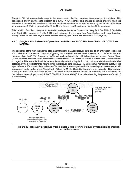
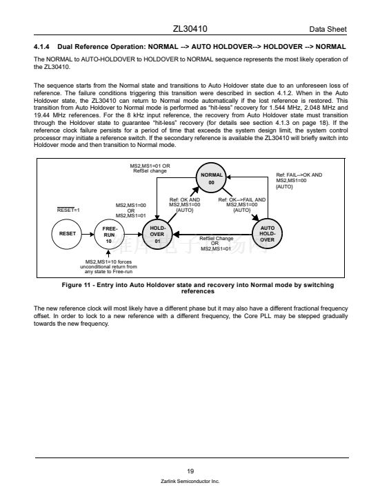
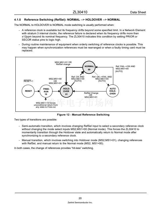
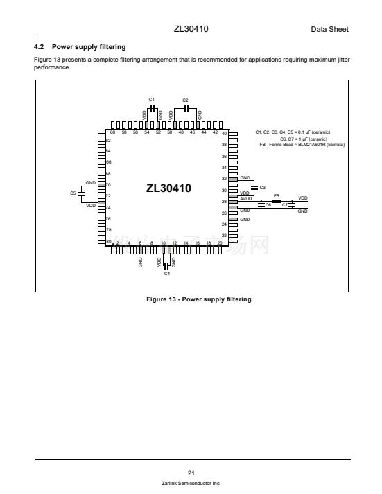
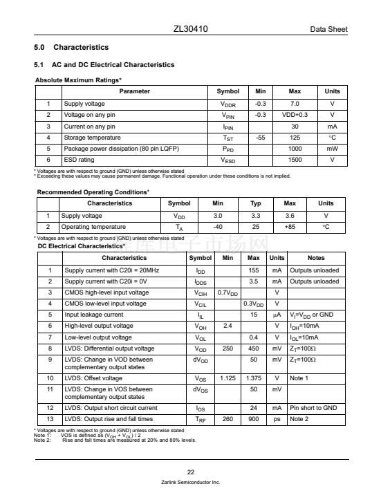
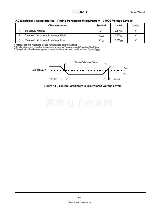
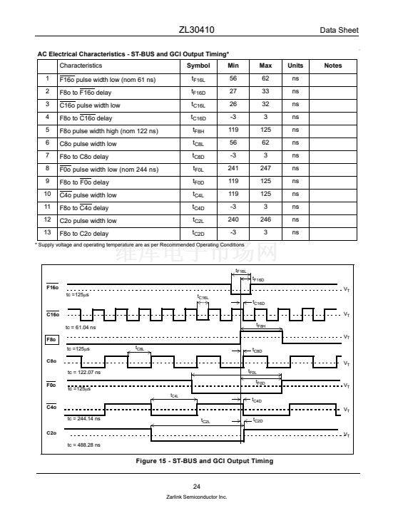
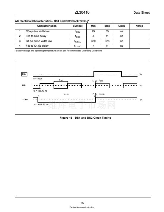
鈥?/div>
Generates clocks for OC-3, STM-1, DS3, E3,
DS2, DS1, E1, 19.44 MHz and ST-BUS
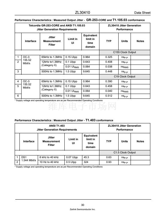
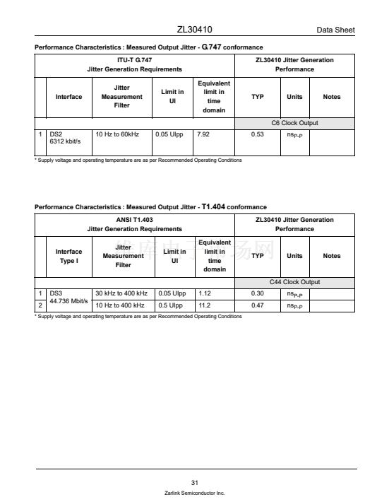
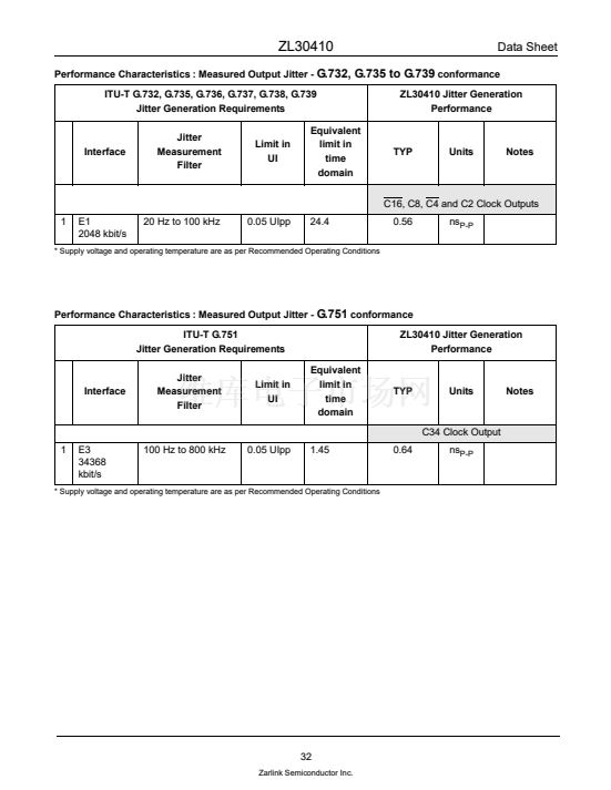
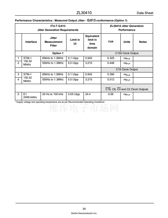
Meets jitter generation requirements for STM-1,
OC-3, DS3, E3, J2 (DS2), E1 and DS1 interfaces
Compatible with GR-253-CORE SONET stratum
3 and G.813 SEC timing compliant clocks
Provides 鈥渉it-less鈥?reference switching
Detects frequency of both reference clocks and
synchronizes to any combination of 8 kHz, 1.544
MHz, 2.048 MHz and 19.44 MHz reference
frequencies
Continuously monitors both references for
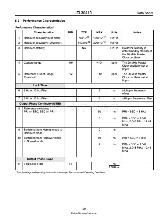
frequency accuracy exceeding 鹵12 ppm
Holdover accuracy of 70x10
-12
meets GR-1244
Stratum 3E and ITU-T G.812 requirements
Meets requirements of G.813 Option 1 for SDH
Equipment Clocks (SEC) and GR-1244 for
Stratum 4E and Stratum 4 Clocks
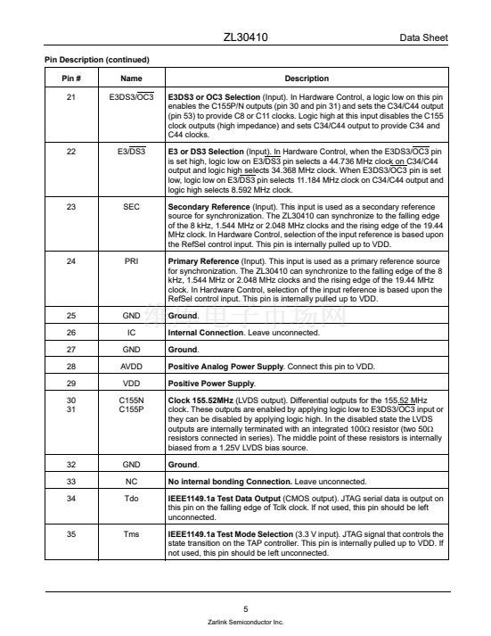
3.3V power supply
Ordering Information
ZL30410QCC
80 Pin LQFP
November 2003
-40擄C to 85擄C
鈥?/div>
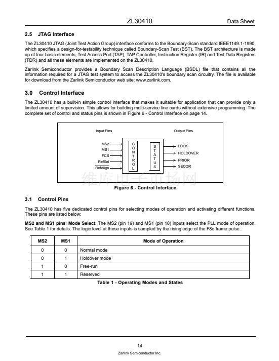
Clock generation for ST-BUS and GCI timing
Description
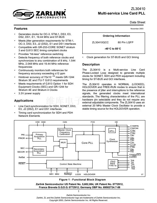
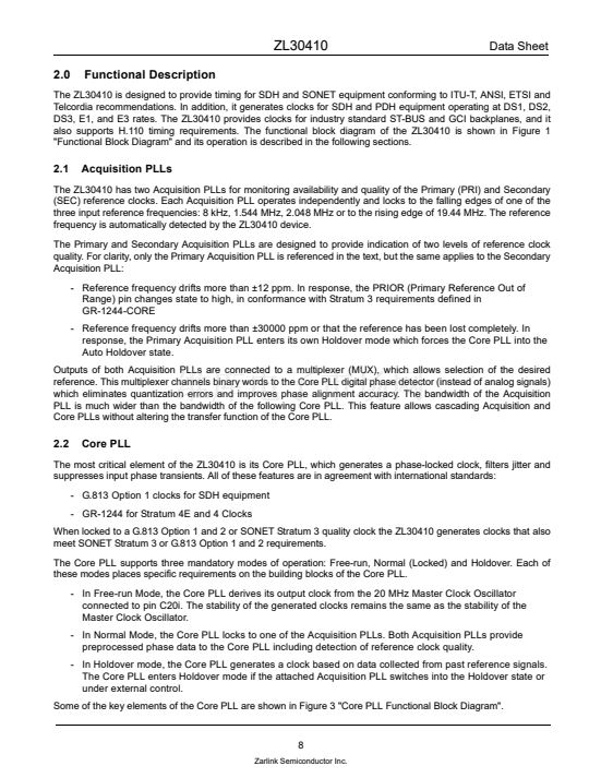
The ZL30410 is a Multi-service Line Card
Phase-Locked Loop designed to generate multiple
clocks for SONET, SDH and PDH equipment including
timing for ST-BUS and GCI interfaces.
The ZL30410 operates in NORMAL (LOCKED),
HOLDOVER and FREE-RUN modes to ensure that in
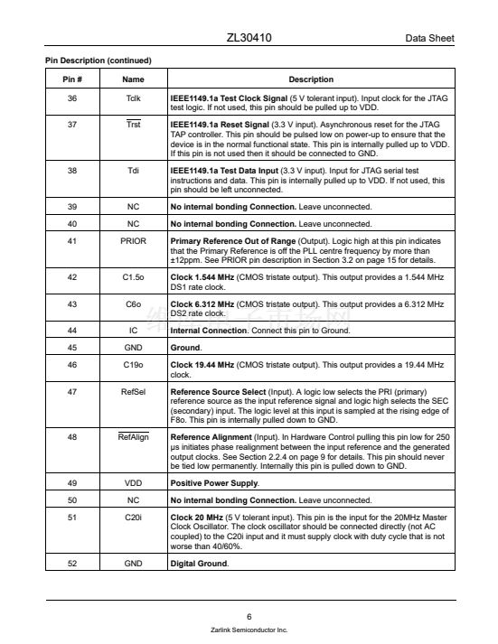
the presence of jitter and interruptions to the reference
signals, the generated clocks meet international
standards. The filtering characteristics of the PLL are
hardware pin selectable and they do not require any
external adjustable components. The ZL30410 uses an
external 20 MHz Master Clock Oscillator to provide a
stable timing source for the HOLDOVER operation.
鈥?/div>
鈥?/div>
鈥?/div>
鈥?/div>
Applications
鈥?/div>
鈥?/div>
Line Card synchronization for SDH, SONET, DS3,
E3, J2 (DS2), E1 and DS1 interfaces
Timing card synchronization for SDH and PDH
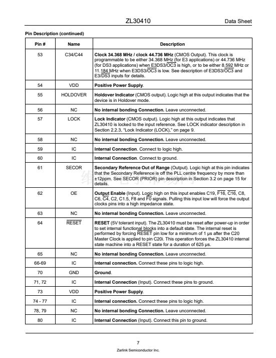
Network Elements
VDD GND
C20i
FCS
OE
PRI
PRIOR
Primary
Acquisition
PLL
Master Clock
Frequency
Calibration
APLL
MUX
SEC
SECOR
RefSel
RESET
Core PLL
Clock
Synthesizer
Secondary
Acquisition
PLL
C155P/N
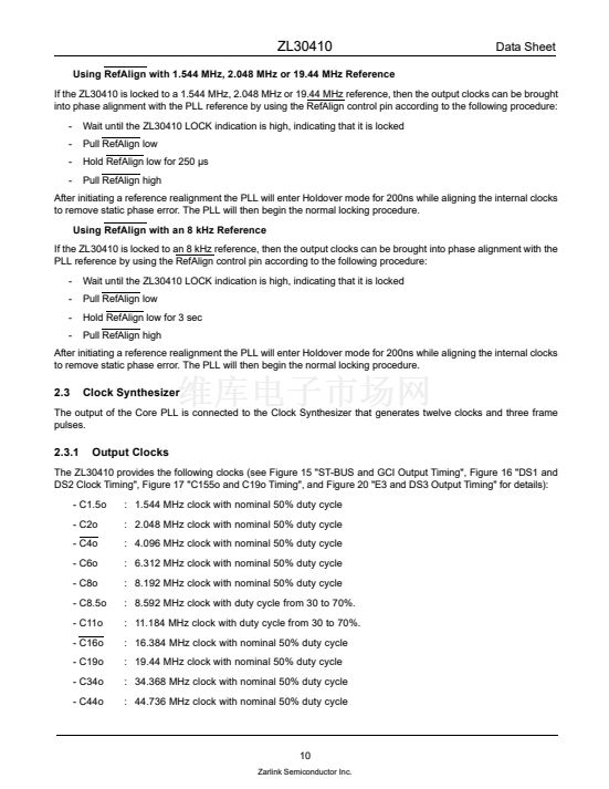
C34/C44
C19o
C16o
C8o
C6o
C4o
C2o
C1.5o
F16o
F8o
F0o
E3DS3/OC3
E3/DS3
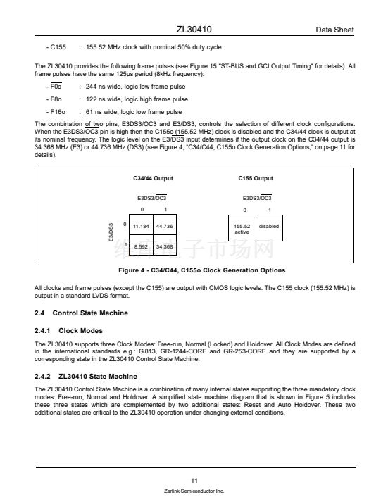
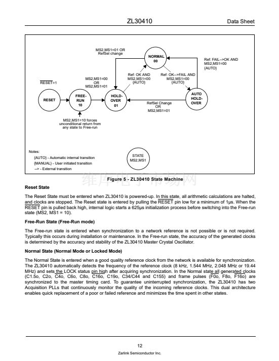
Control State Machine
JTAG
IEEE
1149.1a
Tclk
Tdi
Tdo
Tms
Trst
07
MS1 MS2
RefAlign
LOCK
HOLDOVER
Figure 1 - Functional Block Diagram
Zarlink Semiconductor US Patent No. 5,602,884, UK Patent No. 0772912,
France Brevete S.G.D.G. 0772912; Germany DBP No. 69502724.7-08
1
Zarlink Semiconductor Inc.
Zarlink, ZL and the Zarlink Semiconductor logo are trademarks of Zarlink Semiconductor Inc.
Copyright 2003, Zarlink Semiconductor Inc. All Rights Reserved.
ZL30410相關(guān)型號PDF文件下載
-
型號
版本
描述
廠商
下載
-
英文版
T1/E1 System Synchronizer
-
英文版
T1/E1 System Synchronizer
ZARLINK [Z...
-
英文版
T1/E1 Stratum 3 System Synchronizer
-
英文版
T1/E1 Stratum 3 System Synchronizer
ZARLINK [Z...
-
英文版
T1/E1 Stratum 4/4E Redundant System Clock Synchronizer for D...
-
英文版
T1/E1 Stratum 4/4E Redundant System Clock Synchronizer for D...
ZARLINK [Z...
-
英文版
T1/E1/SDH Stratum 3 Redundant System Clock Synchonizer for A...
-
英文版
T1/E1/SDH Stratum 3 Redundant System Clock Synchonizer for A...
ZARLINK [Z...
-
英文版
SONET/SDH/PDH Network Interface DPLL
-
英文版
SONET/SDH/PDH Network Interface DPLL
ZARLINK [Z...
-
英文版
GbE Line Card Synchronizer
ZARLINK [Z...
-
英文版
Network Interface DPLL
-
英文版
Network Interface DPLL
ZARLINK [Z...
-
英文版
DS1/E1 System Synchronizer with 19.44 MHz Output
-
英文版
DS1/E1 System Synchronizer with 19.44 MHz Output
ZARLINK [Z...
-
英文版
Telecom Rate Conversion DPLL
ZARLINK [Z...
-
英文版
POTS Line Card PLL
ZARLINK [Z...
-
英文版
SONET/SDH OC-48/OC-192 System Synchronizer
ZARLINK [Z...
-
英文版
SONET/SDH OC-48/OC-192 Line Card Synchronizer
ZARLINK [Z...
-
英文版
Low Jitter Line Card Synchronizer
ZARLINK [Z...


 1
1
 2
2
 3
3
 4
4
 5
5
 6
6
 7
7
 8
8
 9
9
 10
10
 11
11
 12
12
 13
13
 14
14
 15
15
 16
16
 17
17
 18
18
 19
19
 20
20
 21
21
 22
22
 23
23
 24
24
 25
25
 26
26
 27
27
 28
28
 29
29
 30
30
 31
31
 32
32
 33
33
 34
34
 35
35
 36
36
 37
37
 38
38
