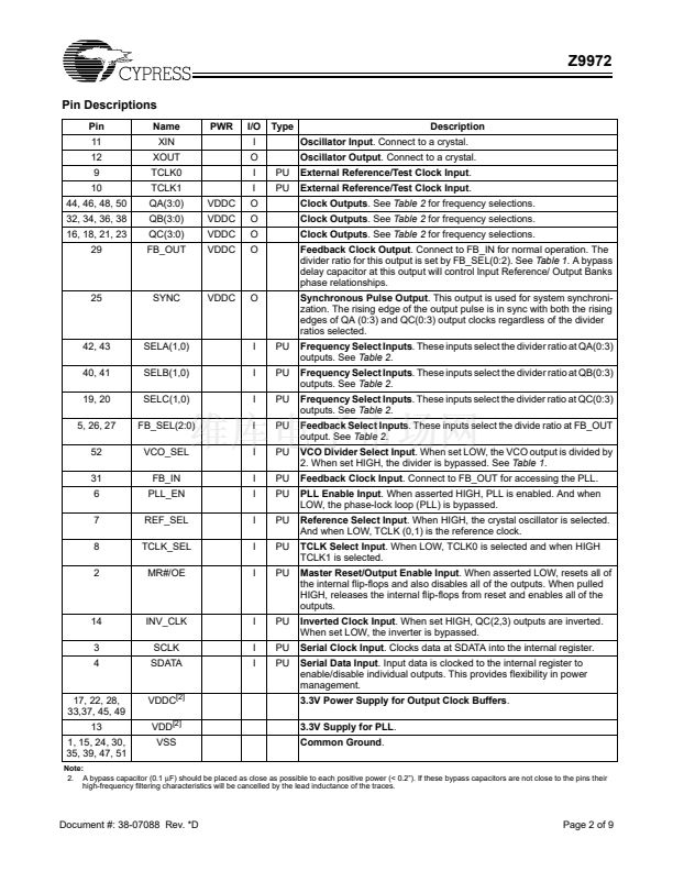
鈥?/div>
Output frequency up to 125 MHz
12 clock outputs: frequency configurable
350 ps max output-to-output skew
Configurable output disable
Two reference clock inputs for dynamic toggling
Oscillator or crystal reference input
Spread Spectrum-compatible
Glitch-free output clocks transitioning
3.3V power supply
Pin-compatible with MPC972
Industrial temperature range: 鈥?0擄C to +85擄C
52-pin TQFP package
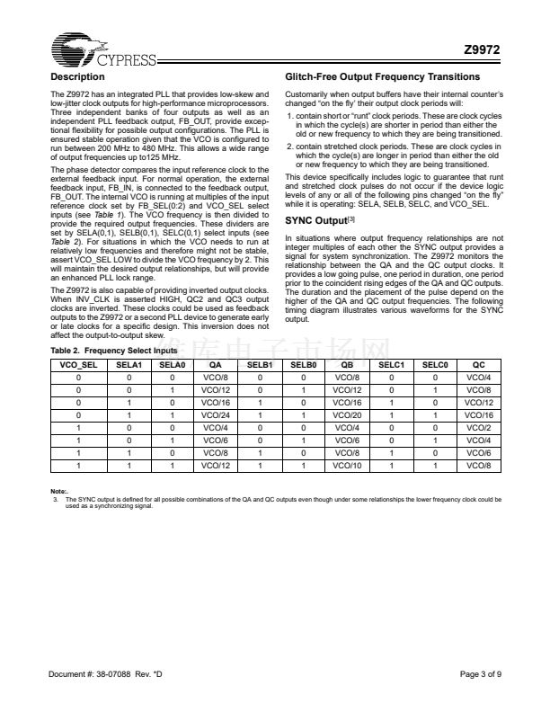
Table 1. Frequency Table
[1]
VCO_SEL FB_SEL2 FB_SEL1 FB_SEL0
0
0
0
0
0
0
0
0
1
1
1
1
1
1
1
1
0
0
0
0
1
1
1
1
0
0
0
0
1
1
1
1
0
0
1
1
0
0
1
1
0
0
1
1
0
0
1
1
0
1
0
1
0
1
0
1
0
1
0
1
0
1
0
1
F
VCO
8x
12x
16x
20x
16x
24x
32x
40x
4x
6x
8x
10x
8x
12x
16x
20x
Note:
1. x = the reference input frequency, 200 MHz < F
VCO
< 480 MHz.
Block Diagram
XIN
XOUT
VCO_SEL
PLL_EN
REF_SEL
D Q
TCLK0
TCLK1
TCLK_SEL
FB_IN
D Q
Sync
Frz
0
1
Phase
Detector
LPF
VCO
0
1
Sync
Frz
QA0
QA1
QA2
QA3
QB0
QB1
FB_SEL2
QB2
QB3
Pin Configuration
SELB1
SELB0
SELA1
SELA0
QA3
VDDC
QA2
VSS
QA1
VDDC
QA0
VSS
VCO_SEL
52 51 50 49 48 47 46 45 44 43 42 41 40
VSS
MR#/OE
SCLK
SDATA
FB_SEL2
PLL_EN
REF_SEL
TCLK_SEL
TCLK0
TCLK1
XIN
XOUT
VDD
1
2
3
4
5
6
7
8
9
10
11
12
13
39
38
37
36
35
34
33
32
31
30
29
28
27
VSS
QB0
VDDC
QB1
VSS
QB2
VDDC
QB3
FB_IN
VSS
FB_OUT
VDDC
FB_SEL0
MR#/OE
Power-On
Reset
SELA(0,1)
SELB(0,1)
SELC(0,1)
FB_SEL(0,1)
SCLK
SDATA
INV_CLK
2
2
2
2
/4, /6, /8, /10
Sync Pulse
Data Generator
D Q
/2
0
1
D Q
D Q
/4, /6, /8, /12
/4, /6, /8, /10
/2, /4, /6, /8
D Q
Sync
Frz
Z9972
QC0
QC1
Sync
Frz
Sync
Frz
Sync
Frz
QC2
QC3
FB_OUT
14 15 16 17 18 19 20 21 22 23 24 25 26
SYNC
FB_SEL1
SYNC
VSS
QC0
VDDC
QC1
SELC0
SELC1
QC2
VDDC
QC3
VSS
INV_CLK
Output Disable
Circuitry
12
Cypress Semiconductor Corporation
Document #: 38-07088 Rev. *D
鈥?/div>
3901 North First Street
鈥?/div>
San Jose
鈥?/div>
CA 95134 鈥?408-943-2600
Revised December 21, 2002


 1
1
 2
2
 3
3
 4
4
 5
5
 6
6
 7
7
 8
8
 9
9
