鈥?/div>
Output phase relationship is precisely controllable
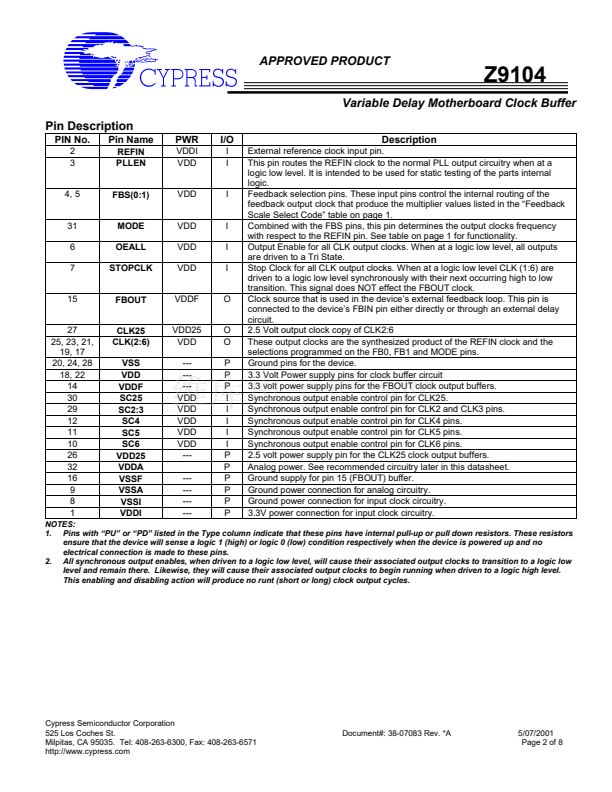
with respect to input clock via a dedicated external
feedback path.
2K volts ESD protected
6 Low Skew Clocks Generated
One 2.5 Volt output clock
Outputs are individually enabled.
Output frequencies from 30 to 100 MHz.
3.3 Volt Vdd operation
Synchronous output enable and disable control
45 - 55% output duty cycle
+/- 100 pSec Cycle to Cycle Jitter
32-Lead TQFP package
Feedback Scale Select Codes
Mode
0
0
0
0
1
1
1
FBS1
0
0
1
1
0
0
1
FBS0
0
1
0
1
0
1
0
Pcounter
梅
4
梅
4
梅
4
梅
8
梅
4
梅
4
梅
4
Ncounter
梅
8
梅
10
梅
12
梅
12
梅
4
梅
5
梅
6
MF*
2.0
2.5
3.0
1.5
1.0
1.25
1.5
1
1
1
梅
8
梅
8
1.0
*Multiplication Factor 鈥?The multiplication factor for
these configurations is the output frequency with
respect to REFIN (FOUT=FIN X multiplication factor)
Block Diagram
MODE
FBS0
FBS1
VDDF
Pin Configuration
VDD25
26
CLK25
27
MODE
SC2,3
VDDA
SC25
32
31
30
29
28
FBIN
REFIN
Ncounter
PLL
1
0
FBOUT
25
CLK2
VSS
Pcounter
PLLEN
Stop
Logic
Stop
Logic
Stop
Logic
Stop
Logic
Stop
Logic
OEALL
STOPCLK
VDD
SC25
CLK25
VDD25
CLK2
SC2,3
CLK3
VDDI
REFIN
PLLEN
FBS0
FBS1
OEALL
STOPCLK
VSSI
1
2
3
4
5
6
7
8
9
Z9104
10
11
12
13
14
15
16
24
23
22
21
20
19
18
17
VSS
CLK3
VDD
CLK4
VSS
CLK5
VDD
CLK6
FBOUT
VSSA
CLK4
CLK5
SC4
SC5
CLK6
SC6
Cypress Semiconductor Corporation
525 Los Coches St.
Milpitas, CA 95035. Tel: 408-263-6300, Fax: 408-263-6571
http://www.cypress.com
Document#: 38-07083 Rev. *A
VDDF
VSSF
FBIN
SC6
SC5
SC4
5/07/2001
Page 1 of 8


 1
1
 2
2
 3
3
 4
4
 5
5
 6
6
 7
7
 8
8
