Composite Transistors
XP06210
(XP6210)
Silicon NPN epitaxial planer transistor
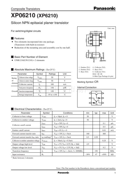
Unit: mm
0.425
1.25鹵0.1
0.425
0.2鹵0.05
For switching/digital circuits
2.1鹵0.1
0.65
G
G
Two elements incorporated into one package.
(Transistors with built-in resistor)
Reduction of the mounting area and assembly cost by one half.
2.0鹵0.1
I
Features
0.65
1
2
3
6
5
4
0.2
0.9鹵0.1
G
0 to 0.1
I
Basic Part Number of Element
UNR1210(UN1210)
脳
2 elements
0.7鹵0.1
0.2鹵0.1
I
Absolute Maximum Ratings
(Ta=25藲C)
Parameter
Symbol
V
CBO
V
CEO
I
C
P
T
T
j
T
stg
Ratings
50
50
100
150
150
鈥?5 to +150
Unit
V
V
mA
mW
藲C
藲C
1 : Emitter (Tr1)
2 : Emitter (Tr2)
3 : Base (Tr2)
Rating Collector to base voltage
of
Collector to emitter voltage
element
Collector current
Total power dissipation
Overall Junction temperature
Storage temperature
4 : Collector (Tr2)
5 : Base (Tr1)
6 : Collector (Tr1)
EIAJ : SC鈥?8
S鈥揗ini Type Package (6鈥損in)
Marking Symbol:
CR
Internal Connection
1
2
3
Tr1
6
5
4
Tr2
I
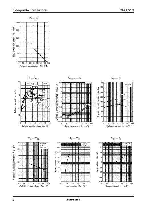
Electrical Characteristics
Parameter
Collector to base voltage
Collector to emitter voltage
Collector cutoff current
Emitter cutoff current
Forward current transfer ratio
Forward current transfer h
FE
ratio
Collector to emitter saturation voltage
Output voltage high level
Output voltage low level
Transition frequency
Input resistance
*1
(Ta=25藲C)
Symbol
V
CBO
V
CEO
I
CBO
I
CEO
I
EBO
h
FE
h
FE
(small/large)
*1
V
CE(sat)
V
OH
V
OL
f
T
R
1
Conditions
I
C
= 10碌A(chǔ), I
E
= 0
I
C
= 2mA, I
B
= 0
V
CB
= 50V, I
E
= 0
V
CE
= 50V, I
B
= 0
V
EB
= 6V, I
C
= 0
V
CE
= 10V, I
C
= 5mA
V
CE
= 10V, I
C
= 5mA
I
C
= 10mA, I
B
= 0.3mA
V
CC
= 5V, V
B
= 0.5V, R
L
= 1k鈩?/div>
V
CC
= 5V, V
B
= 2.5V, R
L
= 1k鈩?/div>
V
CB
= 10V, I
E
= 鈥?mA, f = 200MHz
鈥?0%
150
47
+30%
4.9
0.2
160
0.5
0.99
0.25
V
V
V
MHz
k鈩?/div>
min
50
50
0.1
0.5
0.01
460
typ
max
Unit
V
V
碌A(chǔ)
碌A(chǔ)
mA
Ratio between 2 elements
Note.) The Part number in the Parenthesis shows conventional part number.
0.12
鈥?.02
+0.05
1


 1
1
 2
2
 3
3
