Composite Transistors
XN06534
(XN6534)
Silicon NPN epitaxial planer transistor
For high-frequency amplification
2.90
+0.20
鈥?.05
1.9
鹵0.1
(0.95) (0.95)
4
5
6
1.50
+0.25
鈥?.05
2.8
+0.2
鈥?.3
Unit: mm
0.16
+0.10
鈥?.06
G
3
2
1
(0.65)
0.30
+0.10
鈥?.05
0.50
+0.10
鈥?.05
I
Absolute Maximum Ratings
Parameter
Collector to base voltage
Rating Collector to emitter voltage
of
Emitter to base voltage
element
Collector current
Total power dissipation
Overall Junction temperature
Storage temperature
Symbol
V
CBO
V
CEO
V
EBO
I
C
P
T
T
j
T
stg
(Ta=25藲C)
Ratings
30
20
3
15
200
150
鈥?5 to +150
Unit
V
V
V
mA
mW
藲C
藲C
1 : Collector (Tr1)
2 : Base (Tr1)
3 : Collector (Tr2)
4 : Base (Tr2)
5 : Emitter (Tr2)
6 : Emitter (Tr1)
EIAJ : SC鈥?4
Mini6-G1 Package
Marking Symbol:
7F
Internal Connection
6
5
4
Tr1
1
2
3
Tr2
I
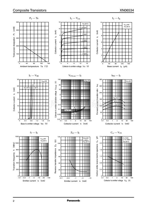
Electrical Characteristics
Parameter
Collector to base voltage
Emitter to base voltage
Forward current transfer ratio
Forward current transfer h
FE
ratio
Base to emitter voltage
Common emitter reverse transfer capacitance
Transition frequency
Noise figure
Power gain
*1
(Ta=25藲C)
Symbol
V
CBO
V
EBO
h
FE
h
FE
(small/large)
*1
V
BE
C
re
f
T
NF
PG
Conditions
I
C
= 10碌A, I
E
= 0
I
E
= 10碌A, I
C
= 0
V
CB
= 6V, I
E
= 鈥?mA
V
CB
= 6V, I
E
= 鈥?mA
V
CB
= 6V, I
E
= 鈥?mA
V
CB
= 6V, I
E
= 鈥?mA, f = 10.7MHz
V
CB
= 6V, I
E
= 鈥?mA, f = 200MHz
V
CB
= 6V, I
E
= 鈥?mA, f = 100MHz
V
CB
= 6V, I
E
= 鈥?mA, f = 100MHz
450
min
30
3
40
0.5
0.99
720
0.8
650
3.3
24
1
mV
pF
MHz
dB
dB
260
typ
max
Unit
V
V
Ratio between 2 elements
Note) The Part number in the Parenthesis shows conventional part number.
0 to 0.1
1.1
+0.3
鈥?.1
G
1.1
+0.2
鈥?.1
I
Basic Part Number of Element
2SC2404
脳
2 elements
10擄
5擄
G
Two elements incorporated into one package.
Reduction of the mounting area and assembly cost by one half.
0.4
鹵0.2
I
Features
1


 1
1
 2
2
 3
3
