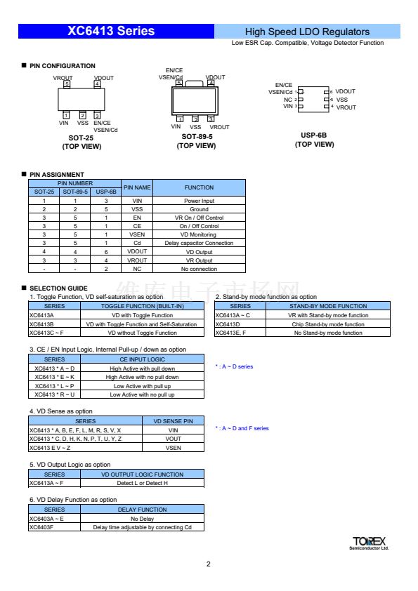
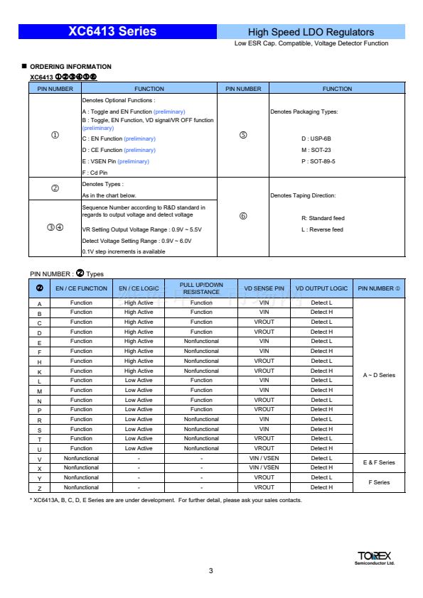
XC6413 Series
High Speed LDO Regulators
Low ESR Cap. Compatible, Voltage Detector Function
July 15, 2003 Ver. 1
!
Low Power Consumption
!
Dropout Voltage
!
Maximum Output Current
!
Highly Accurate
!
VR Setting Output Voltage Range
!
Detect Voltage Setting Range
!
Low ESR capacitor compatible
: 35碌A(chǔ) (TYP.)
: 60mV @ 30mA
: 200mV @ 100mA
: more than 300mA (380mA limit)
(1.8V鈮ROUT鈮?.3V)
:
鹵
2%
: 0.9V ~ 5.5V
: 0.9V ~ 6.0V (VIN :
鈮?.0V)
"
APPLICATIONS
#
#
#
#
#
#
#
Mobile phones, Cordless phones
Wireless communication equipment
Cameras, Video recorders
Portable games
Portable AV equipment
Reference voltage
Battery powered equipment
"
GENERAL DESCRIPTION
The XC6413 series are highly precise, low noise, positive voltage LDO
regulators with voltage detector manufactured using CMOS processes.
More the series achieves high ripple rejection and low dropout and
consists of a voltage reference, an error amplifier, a current limiter and a
phase compensation circuit plus a driver transistor. Detect voltage is
selectable in 0.1V increments within a range of 0.9V ~ 6.0V and VR
output voltage is selectable within a range of 0.9V~5.5V.
The series is also compatible with low ESR ceramic capacitors which
give added output stability. This stability can be maintained even during
load fluctuations due to the excellent transient response of the series.
The current limiter's foldback circuit also operates as a short protect for
the output current limiter and the output pin.
The series provides options to choose suited functions to each systems
such as detector monitoring, detector output logic, CE and EN pin input
logic, internal pull-up / down resistance, power ready (PR) function.
The IC's internal regulator circuitry can be in stand-by mode by the EN
function with the XC6413 A to C series.
The whole IC's circuitry can be in stand-by mode via CE function with the
XC6413D series (semi-custom). In the stand by mode, power
consumption can be greatly reduced.
XC6413 A and B series has toggle operation function. The regulator
output can be OFF when XC6413B series detect voltage (semi-custom).
XC6413E series can monitor the other power source by using VSEN pin
(semi-custom).
By the function to delay capacitor, XC6413F series can delay VD output.
Delay time can be regulated by a capacitor (semi-custom).
Options setup of detector monitoring, detector output logic, CE/EN pin
input logic, internal pull-up and pull-down resistance etc. are possible.
The function such as Power Ready (PR) function which suited systems,
can be chosen (semi-custom).
"
FEATURES
Maximum Output Current
: more than 300mA
(380mA limit)
(1.8V鈮ROUT鈮?.3V)
Dropout Voltage
Maximum Operating Voltage
VR Setting Output Voltage Range
VD Detect Voltage Setting Range
When monitoring VIN
VR setting voltage accuracy
VD detect voltage accuracy
VR.VD Temperature Coefficient
Low Power Consumption
High Ripple Rejection
Low Output Noise
Low ESR Capacitor Compatible
Ultra Small Packages
: 200mV (IROUT=100mA)
: 2.0V ~ 10.0V
: 0.9V~ 5.5V (0.1V step)
: 0.9V ~ 6.0V (0.1V step)
: more than 2.0V
: 鹵 2%
: 鹵 2%
: 鹵100ppm/
O
C (TYP.)
: TYP. 35碌A(chǔ)
: 65dB (10kHz)
: 30mVrms
: Ceramic capacitor
: SOT-25 (SOT-23-5)
: USP-6B
: SOT-89-5
Operational Ambient Temperature:
: - 40 ~ 85
O
C
"
TYPICAL APPLICATIONS
1
CI
1碌
V
IN
V
SS
VR
OUT
5
Rpull
220K
CL
1碌F
1
C
IN
1碌F
V
IN
V
SS
V
SEN
VR
OUT
5
Rpull
220K
VD
OUT
4
CL
1碌F
C
IN
1碌F
1
2
3
V
I
VR
OUT
5
Rpull
220K
CL
1碌F
2
3
2
3
V
SS
Cd
EN/CE
VD
OUT
4
VD
OUT
4
Cd
0.01碌F
XC6413A ~ D Series
XC6413E Series
XC6413F Series
Semiconductor Ltd.
1


 1
1
 2
2
 3
3
 4
4
 5
5
 6
6
 7
7
 8
8
 9
9
 10
10
 11
11
 12
12
 13
13
