鈥?/div>
In-system programmable 3.3V PROMs for configuration
of Xilinx FPGAs
- Endurance of 10,000 program/erase cycles
- Program/erase over full commercial voltage and
temperature range
IEEE Std 1149.1 boundary-scan (JTAG) support
Simple interface to the FPGA; could be configured to
use only one user I/O pin
Cascadable for storing longer or multiple bitstreams
Dual configuration modes
- Serial Slow/Fast configuration (up to 15 mHz).
- Parallel
Low-power advanced CMOS FLASH process
5 V tolerant I/O pins accept 5 V, 3.3 V and 2.5 V signals.
3.3 V or 2.5 V output capability
Available in PC20, SO20, PC44 and VQ44 packages.
Design support using the Xilinx Alliance and
Foundation series software packages.
JTAG command initiation of standard FPGA
configuration.
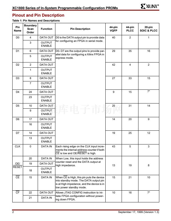
Description
Xilinx introduces the XC1800 series of in-system program-
mable configuration PROMs. Initial devices in this 3.3V
family are a 4 megabit, a 2 megabit, a 1 megabit, a 512
Kbit, a 256 Kbit, and a 128 Kbit PROM that provide an
easy-to-use, cost-effective method for re-programming and
storing large Xilinx FPGA or CPLD configuration bit-
streams.
When the FPGA is in Master Serial mode, it generates a
configuration clock that drives the PROM. A short access
time after the rising CCLK, data is available on the PROM
DATA (D0) pin that is connected to the FPGA DIN pin. The
FPGA generates the appropriate number of clock pulses to
complete the configuration. When the FPGA is in Slave
Serial mode, the PROM and the FPGA are clocked by an
external clock.
When the FPGA is in Express or SelectMAP Mode, an
external oscillator will generate the configuration clock that
drives the PROM and the FPGA. After the rising CCLK
edge, data are available on the PROM鈥檚 DATA (D0-D7)
pins. The data will be clocked into the FPGA on the follow-
ing rising edge of the CCLK. Neither Express nor Select-
MAP utilize a Length Count, so a free-running oscillator
may be used. See
Figure 5
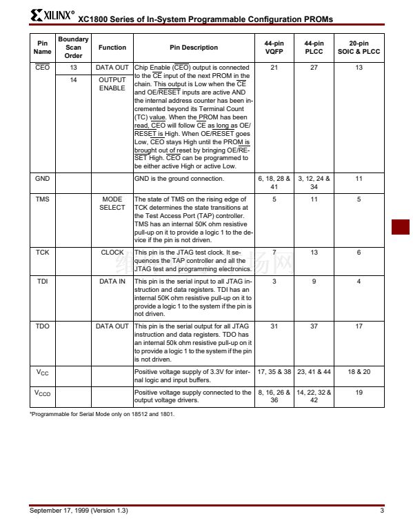
Multiple devices can be concatenated by using the CEO
output to drive the CE input of the following device. The
clock inputs and the DATA outputs of all PROMs in this
chain are interconnected. All devices are compatible and
can be cascaded with other members of the family or with
the XC1700L one-time programmable Serial PROM family.
CLK CE
OE/Reset
鈥?/div>
鈥?/div>
鈥?/div>
鈥?/div>
鈥?/div>
鈥?/div>
鈥?/div>
鈥?/div>
鈥?/div>
鈥?/div>
TCK
TMS
TDI
TDO
Control
and
JTAG
Interface
Data
Memory
Address
Data
Serial
or
Parallel
Interface
CEO
D0 DATA
(Serial or Parallel
(Express/SelectMAP)
Mode)
D1 - D7
Express Mode and
SelectMAP Interface
CF
99020300
Figure 1: XC1800 Series Block Diagram
September 17, 1999 (Version 1.3)
1
XC1800相關(guān)型號PDF文件下載
-
型號
版本
描述
廠商
下載
-
英文版
XC1800 Series of In-System Programmable Configuration PROMs
-
英文版
XC1800 Series of In-System Programmable Configuration...
XILINX [Xi...
-
英文版
In-System Programmable Configuration PROMs
-
英文版
In-System Programmable Configuration PROMs
XILINX [Xi...
-
英文版
C,SERIAL EEPROM,NOR FLASH,CMOS,TQFP,44PIN,PLASTIC
-
英文版
IC,SERIAL EEPROM,NOR FLASH,CMOS,TQFP,44PIN,PLASTIC
-
英文版
In-System-Programmable Configuration PROMs
XILINX [Xi...
-
英文版
In-System Programmable Configuration PROMs
-
英文版
In-System Programmable Configuration PROMs
XILINX [Xi...
-
英文版
In-System Programmable Configuration PROMs
-
英文版
In-System Programmable Configuration PROMs
XILINX [Xi...
-
英文版
In-System Programmable Configuration PROMs
-
英文版
In-System Programmable Configuration PROMs
XILINX [Xi...
-
英文版
In-System Programmable Configuration PROMs
-
英文版
In-System Programmable Configuration PROMs
XILINX [Xi...
-
英文版
In-System Programmable Configuration PROMs
-
英文版
In-System Programmable Configuration PROMs
XILINX [Xi...
-
英文版
In-System Programmable Configuration PROMs
-
英文版
In-System Programmable Configuration PROMs
XILINX [Xi...
-
英文版
In-System Programmable Configuration PROMs


 1
1
 2
2
 3
3
 4
4
 5
5
 6
6
 7
7
 8
8
 9
9
 10
10
 11
11
 12
12
 13
13
 14
14
 15
15
 16
16
