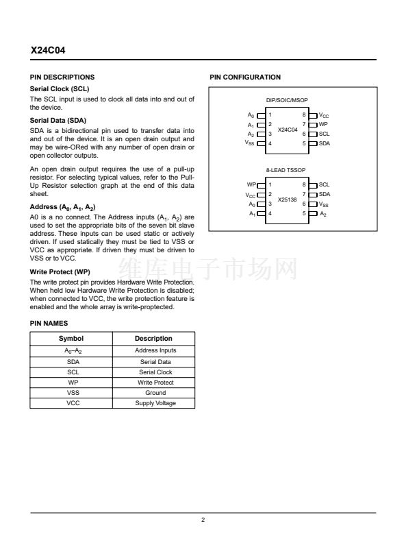
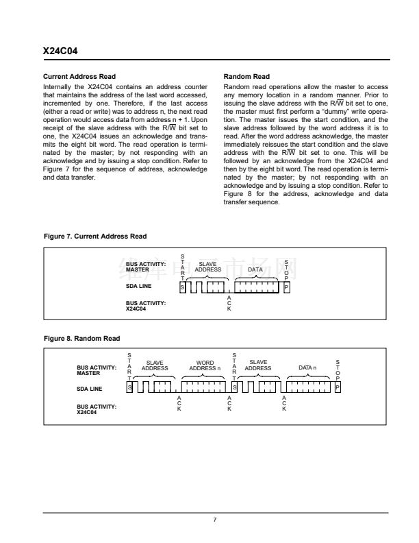
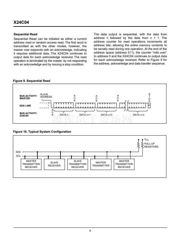
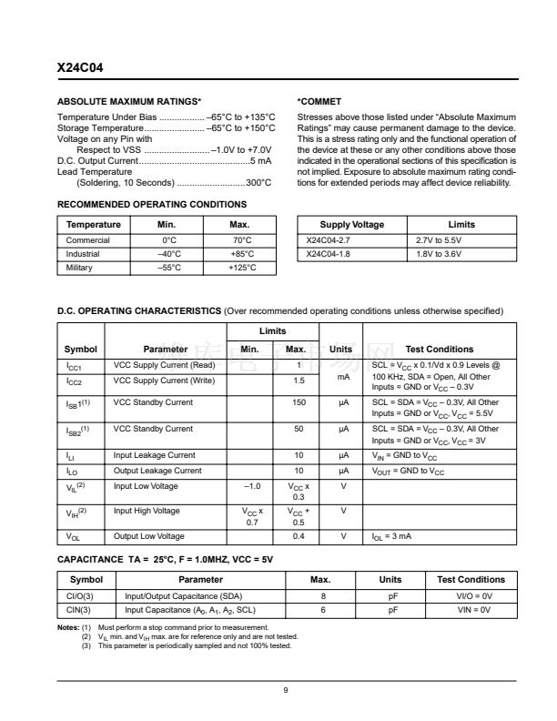
鈥?/div>
1.8V to 3.6V, 2.7V to 5.5V Power Supply Versions
Low Power CMOS
鈥擜ctive Read Current Less Than 1 mA
鈥擜ctive Write Current Less Than 1.5 mA
鈥擲tandby Current Less Than 1 碌A
Internally Organized 512 x 8
2 Wire Serial Interface
鈥擝idirectional Data Transfer Protocol
鈥擲chmitt Trigger Input Noise Suppression
400Khz across VCC range
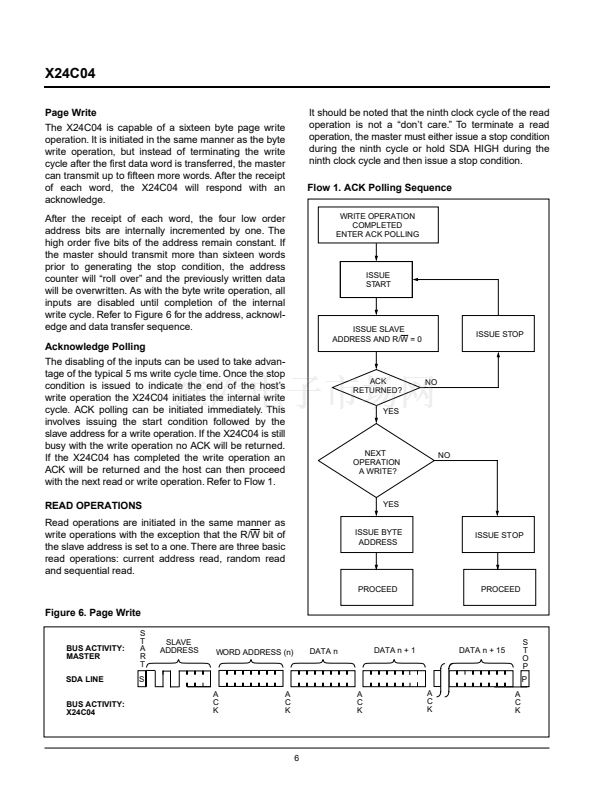
Sixteen Byte Page Write Mode
鈥擬inimizes Total Write Time Per Byte
Self Timed Write Cycle
鈥擳ypical Write Cycle Time of 5 ms
High Reliability
鈥擡ndurance: 100,000 Cycles
鈥擠ata Retention: 100 Years
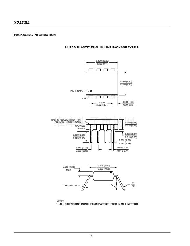
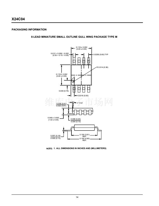
8 Pin Mini-DIP, 8 Pin SOIC, 8 pin MSOP and
8 pin TSSOP
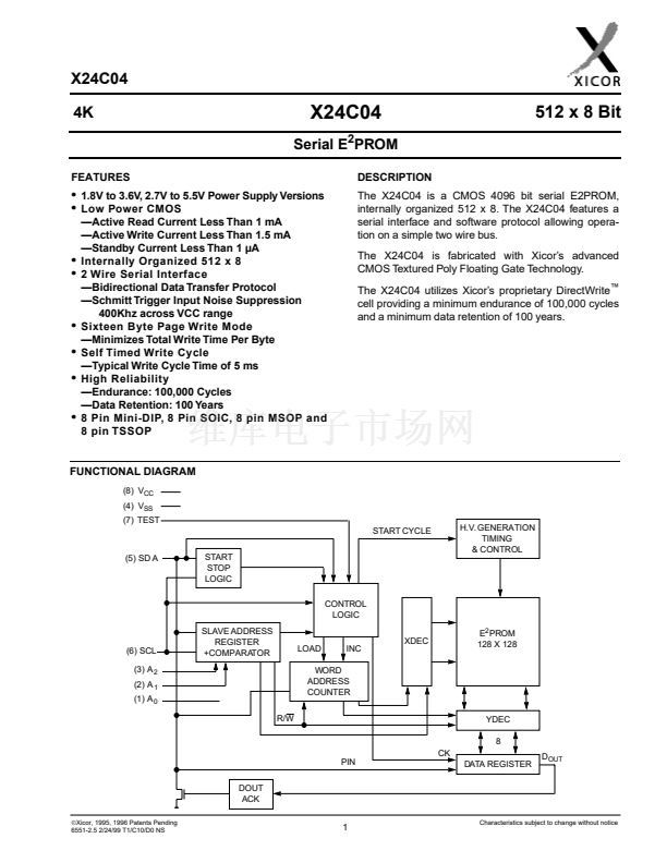
FUNCTIONAL DIAGRAM
(8) V
CC
(4) V
SS
(7) TEST
START CYCLE
(5) SD A
START
STOP
LOGIC
CONTROL
LOGIC
SLAVE ADDRESS
REGISTER
+COMPARATOR
XDEC
E
2
PROM
128 X 128
H.V. GENERATION
TIMING
& CONTROL
(6) SCL
(3) A
2
(2) A
1
(1) A
0
LOAD
INC
WORD
ADDRESS
COUNTER
R/W
YDEC
8
CK
PIN
DOUT
ACK
DATA REGISTER
D
OUT
脫
Xicor, 1995, 1996 Patents Pending
6551-2.5 2/24/99 T1/C10/D0 NS
1
Characteristics subject to change without notice


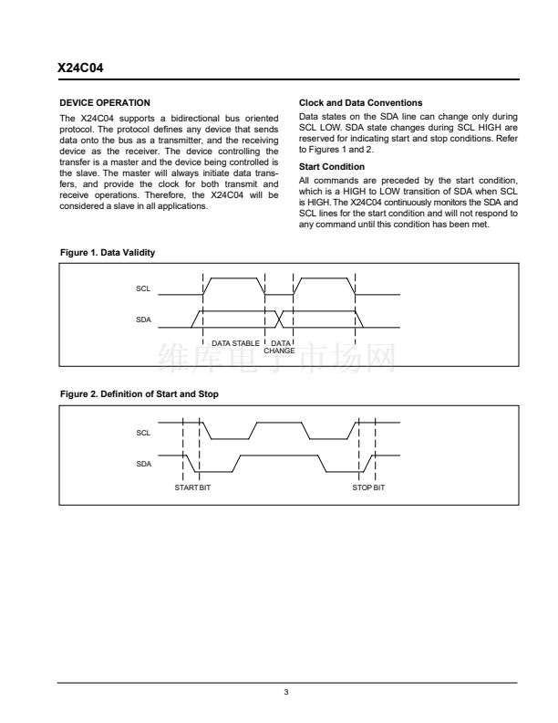
 1
1
 2
2
 3
3
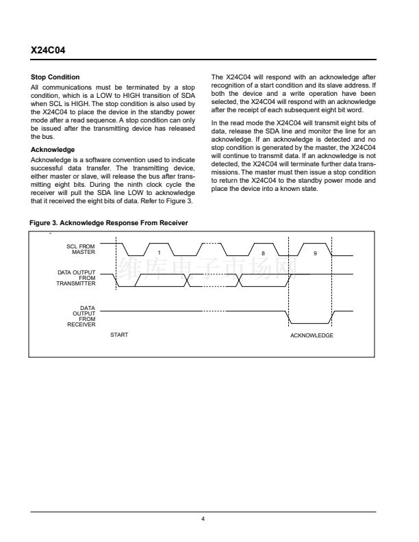 4
4
 5
5
 6
6
 7
7
 8
8
 9
9
 10
10
 11
11
 12
12
 13
13
 14
14
 15
15
 16
16
