WF8M32-XG4DX5
HI-RELIABILITY PRODUCT
8Mx32 5V FLASH MODULE
FEATURES
s
Access Time of 100, 120, 150ns
s
Packaging:
ADVANCED*
s
s
s
s
s
s
鈥?68 Lead, 40 mm (1.560") square hermetic CQFP, 5.2 mm
(0.205") high (Package 503)
Sector Architecture
鈥?32 equal size sectors of 64KBytes per each 2Mx8 chip
鈥?Any combination of sectors can be erased. Also supports
full chip erase.
100,000 Write/Erase Cycles Minimum
Organized as 8Mx32
Commercial, Industrial, and Military Temperature Ranges
5 Volt Read and Write. 5V
鹵
10% Supply.
Low Power CMOS
s
Data Polling and Toggle Bit feature for detection of program
or erase cycle completion.
s
Supports reading or programming data to a sector not being
erased.
s
RESET pin resets internal state machine to the read mode.
(Not available in HIP package for WF2M32-XHX5)
s
Built-in Decoupling Caps and Multiple Ground Pins for Low
Noise Operation, Seperate Power and Ground Planes to
improve noise immunity.
s
Built in Buffering.
* This data sheet describes a product that may or may not be under
development, and is subject to change or cancellation without notice.
Note: For programming information refer to Flash Programming 16M5
Application Note.
FIG. 1
PIN CONFIGURATION FOR WF8M32-XG4DX5
TOP VIEW
NC
A
0
A
1
A
2
A
3
A
4
A
5
CS
1
GND
CS
3
WE
A
6
A
7
A
8
A
9
A
10
V
CC
PIN DESCRIPTION
I/O
0-31
A
0-22
Data Inputs/Outputs
Address Inputs
Write Enable
Chip Selects
Output Enable
Power Supply
Reset
Ground
Not Connected
9 8 7 6 5 4 3 2 1 68 67 66 65 64 63 62 61
I/O
0
I/O
1
I/O
2
I/O
3
I/O
4
I/O
5
I/O
6
I/O
7
GND
I/O
8
I/O
9
I/O
10
I/O
11
I/O
12
I/O
13
I/O
14
I/O
15
10
11
12
13
14
15
16
17
18
19
20
21
22
23
24
25
26
27 28 29 30 31 32 33 34 35 36 37 38 39 40 41 42 43
60
59
58
57
56
55
54
53
52
51
50
49
48
47
46
45
44
I/O
16
I/O
17
I/O
18
I/O
19
I/O
20
I/O
21
I/O
22
I/O
23
GND
I/O
24
I/O
25
I/O
26
I/O
27
I/O
28
I/O
29
I/O
30
I/O
31
WE
CS
1-4
OE
V
CC
RESET
GND
NC
BLOCK DIAGRAM
Interface
RESET
CS
1-4
WE
OE
A
0-22
1
4
1
1
23
1
4
1
1
23
CS
1
2M x 8
CS
2
2M x 8
2M x 8
2M x 8
2M x 8
I/O
8-15
8
CS
3
2M x 8
2M x 8
2M x 8
2M x 8
I/O
16-23
8
CS
4
2M x 8
2M x 8
2M x 8
2M x 8
I/O
24-31
8
V
CC
A
11
A
12
A
13
A
14
A
15
A
16
CS
2
OE
CS
4
A
17
A
18
A
19
A
20
RESET
A21
A22
2M x 8
2M x 8
2M x 8
I/O
0-7
8
32
I/O
0-31
CS
1
selects I/O
0-7
, CS
2
selects I/O
8-15
, CS
3
selects I/O
16-23
, CS
4
selects I/O
24-31
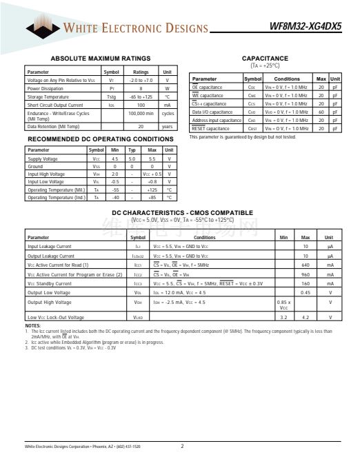
October 1999 Rev. 3
1
White Electronic Designs Corporation 鈥?(602) 437-1520 鈥?www.whiteedc.com


 1
1
 2
2
 3
3
 4
4
 5
5
 6
6
 7
7
 8
8
 9
9
 10
10
