White Electronic Designs
2Mx32 5V Flash Module
FEATURES
Access Time of 90, 120, 150ns
Packaging:
鈥?66 pin, PGA Type, 1.185" square, Hermetic
Ceramic HIP (Package 401).
鈥?68 lead, Hermetic CQFP (G2U), 22.4mm
(0.880") square (Package 510) 3.56mm
(0.140") height. Designed to fit JEDEC 68 lead
0.990" CQFJ footprint (Fig. 3)
Sector Architecture
鈥?32 equal size sectors of 64KBytes per each
2Mx8 chip
鈥?Any combination of sectors can be erased.
Also supports full chip erase.
Minimum 100,000 Write/Erase Cycles Minimum
Organized as 2Mx32
PRELIMINARY*
WF2M32-XXX5
Commercial, Industrial, and Military
Temperature Ranges
5 Volt Read and Write. 5V 鹵 10% Supply.
Low Power CMOS
Data Polling and Toggle Bit feature for detection
of program or erase cycle completion.
Supports reading or programming data to a
sector not being erased.
RESET pin resets internal state machine to the
read mode.
Built in Decoupling Caps and Multiple Ground
Pins for Low Noise Operation, Separate Power
and Ground Planes to improve noise immunity
* This data sheet describes a product under development, not fully characterized,
and is subject to change without notice.
Note:
For programming information refer to Flash Programming 16M5 Application
Note.
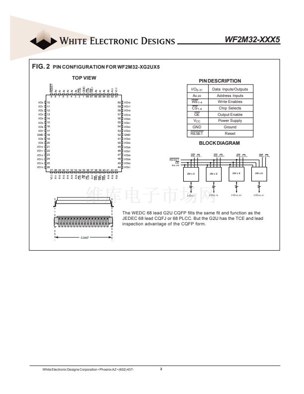
FIG. 1
PIN CONFIGURATION FOR WF2M32-XHX5
TOP VIEW
PIN DESCRIPTION
I/O0-31
A
0-20
WE
1-4
CS
1-4
OE
VCC
GND
Data Inputs/Outputs
Address Inputs
Write Enables
Chip Selects
Output Enable
Power Supply
Ground
1
I/O
8
I/O
9
I/O
10
A
14
A
16
A
11
A
0
A
18
I/O
0
I/O
1
I/O
2
11
12
WE
2
CS
2
GND
I/O
11
A
10
A
9
A
15
V
CC
CS
1
A
19
I/O
3
22
23
I/O
15
I/O
14
I/O
13
I/O
12
OE
A
17
WE
1
I/O
7
I/O
6
I/O
5
I/O
4
33
I/O
24
I/O
25
I/O
26
A
7
A
12
A
20
A
13
A
8
I/O
16
I/O
17
I/O
18
34
V
CC
CS
4
WE
4
I/O
27
A
4
A
5
A
6
WE
3
CS
3
GND
I/O
19
44
45
I/O
31
I/O
30
I/O
29
I/O
28
A
1
A
2
A
3
I/O
23
I/O
22
I/O
21
I/O
20
55
56
BLOCK DIAGRAM
W E
1
CS
1
OE
A
0
-
20
2M x 8
2M x 8
W E
2
CS
2
W E
3
CS
3
W E
4
CS
4
2M x 8
2M x 8
8
8
8
8
I/O
0-7
I/O
8-15
I/O
16-23
I/O
24-31
66
RESET internally tied to Vcc in the HIP package for this pin
configuration. See Alternate Pin Configuration with RESET tied
to pin 12 for system control of reset (Fig. 10, page 11).
January 2004 Rev.4
1
White Electronic Designs Corporation 鈥?(602) 437-1520 鈥?/div>
next


 1
1
 2
2
 3
3
 4
4
 5
5
 6
6
 7
7
 8
8
 9
9
 10
10
 11
11
 12
12
 13
13
 14
14
