WF1M32B-XXX3
HI-RELIABILITY PRODUCT
1Mx32 3.3V FLASH MODULE
FEATURES
s
Access Times of 100, 120, 150ns
s
Packaging
鈥?66 pin, PGA Type, 1.185" square, Hermetic Ceramic
HIP (Package 401)
鈥?68 lead, Low Profile CQFP (G2T), 4.6mm (0.180")
square (Package 509)
s
1,000,000 Erase/Program Cycles
s
Sector Architecture
鈥?One 16KByte, two 8KBytes, one 32KByte, and fifteen
64kBytes in byte mode
鈥?Any combination of sectors can be concurrently erased.
Also supports full chip erase
s
Organized as 1Mx32
s
Commercial, Industrial and Military Temperature Ranges
s
3.3 Volt for Read and Write Operations
Note: For programming information refer to Flash Programming 8M3
Application Note.
s
Boot Code Sector Architecture (Bottom)
s
Low Power CMOS, 1.0mA Standby
s
Embedded Erase and Program Algorithms
s
Built-in Decoupling Caps for Low Noise Operation
s
Erase Suspend/Resume
鈥?Supports reading data from or programing data to a
sector not being erased
s
Low Current Consumption
Typical values at 5MHz:
鈥?40mA Active Read Current
鈥?80mA Program/Erase Current
s
Weight
WF1M32B-XG2TX3 -8 grams typical
WF1M32B-XHX3 -13 grams typical
PIN CONFIGURATION FOR WF1M32B-XHX3
TOP VIEW
1
I/O
8
I/O
9
I/O
10
A
14
A
16
A
11
A
0
A
18
I/O
0
I/O
1
I/O
2
11
22
12
RESET
CS
2
GND
I/O
11
A
10
A
9
A
15
V
CC
CS
1
A
19
I/O
3
33
23
I/O
15
I/O
14
I/O
13
I/O
12
OE
A
17
WE
I/O
7
I/O
6
I/O
5
I/O
4
I/O
24
I/O
25
I/O
26
A
7
A
12
NC
A
13
A
8
I/O
16
I/O
17
I/O
18
44
34
V
CC
CS
4
NC
I/O
27
A
4
A
5
A
6
NC
CS
3
GND
I/O
19
55
45
I/O
31
I/O
30
I/O
29
I/O
28
A
1
56
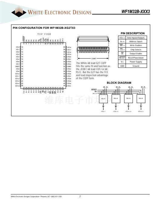
PIN DESCRIPTION
I/O
0-31
A
0-19
WE
CS
1-4
OE
RESET
V
CC
A
2
A
3
I/O
23
I/O
22
I/O
21
I/O
20
66
1M x 8
1M x 8
1M x 8
1M x 8
RESET
WE
OE
A
0
-
19
Data Inputs/Outputs
Address Inputs
Write Enable
Chip Selects
Output Enable
Reset
Power Supply
Ground
Not Connected
GND
NC
BLOCK DIAGRAM
CS
1
CS
2
CS
3
CS
4
8
8
8
8
I/O
0-7
I/O
8-15
I/O
16-23
I/O
24-31
May 1999 Rev. 4
1
White Electronic Designs Corporation 鈥?Phoenix, AZ 鈥?(602) 437-1520


 1
1
 2
2
 3
3
 4
4
 5
5
 6
6
 7
7
 8
8
 9
9
 10
10
 11
11
 12
12
 13
13
