WEDPN16M72V-XBX
16Mx72 Synchronous DRAM
FEATURES
!
High Frequency = 100, 125MHz
!
Package:
GENERAL DESCRIPTION
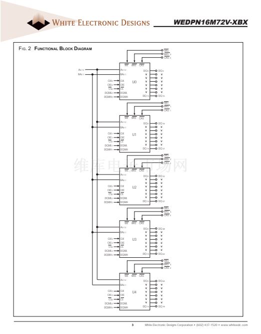
The 128MByte (1Gb) SDRAM is a high-speed CMOS, dynamic
random-access, memory using 5 chips containing 268,435,456
bits. Each chip is internally configured as a quad-bank DRAM with
a synchronous interface. Each of the chip鈥檚 67,108,864-bit banks
is organized as 8,192 rows by 512 columns by 16 bits.
Read and write accesses to the SDRAM are burst oriented;
accesses start at a selected location and continue for a pro-
grammed number of locations in a programmed sequence.
Accesses begin with the registration of an ACTIVE command,
which is then followed by a READ or WRITE command. The
address bits registered coincident with the ACTIVE command
are used to select the bank and row to be accessed (BA0, BA1
select the bank; A0-12 select the row). The address bits regis-
tered coincident with the READ or WRITE command are used to
select the starting column location for the burst access.
The SDRAM provides for programmable READ or WRITE burst
lengths of 1, 2, 4 or 8 locations, or the full page, with a burst
terminate option. An AUTO PRECHARGE function may be en-
abled to provide a self-timed row precharge that is initiated at the
end of the burst sequence.
The 1Gb SDRAM uses an internal pipelined architecture to achieve
high-speed operation. This architecture is compatible with the 2n
rule of prefetch architectures, but it also allows the column address
to be changed on every clock cycle to achieve a high-speed, fully
random access. Precharging one bank while accessing one of the
other three banks will hide the precharge cycles and provide seam-
less, high-speed, random-access operation.
The 1Gb SDRAM is designed to operate in 3.3V, low-power
memory systems. An auto refresh mode is provided, along with
a power-saving, power-down mode.
鈥?219 Plastic Ball Grid Array (PBGA), 32 x 25mm
!
Single 3.3V 鹵0.3V power supply
!
Fully Synchronous; all signals registered on positive edge
of system clock cycle
!
Internal pipelined operation; column address can be
changed every clock cycle
!
Internal banks for hiding row access/precharge
!
Programmable Burst length 1,2,4,8 or full page
!
8192 refresh cycles
!
Commercial, Industrial and Military Temperature Ranges
!
Organized as 16M x 72
!
Weight: WEDPN16M72V-XBX - 2.5 grams typical
BENEFITS
!
40% SPACE SAVINGS
!
Reduced part count
!
Reduced I/O count
鈥?19% I/O Reduction
!
Reduced trace lengths for lower parasitic capacitance
!
Suitable for hi-reliability applications
!
Laminate interposer for optimum TCE match
!
Upgradeable to 32M x 72 density (contact factory for
information)
* The a product that is subject to change without notice.
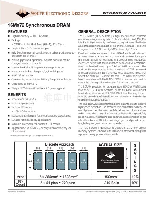
Discrete Approach
11.9
11.9
11.9
11.9
11.9
ACTUAL SIZE
22.3
54
TSOP
54
TSOP
54
TSOP
54
TSOP
54
TSOP
25
White Electronic Designs
WEDPN16M72V-XBX
32
S
A
V
I
N
G
S
40%
19%
Area
I/O
Count
November 2003 Rev. 6
5 x 265mm
2
= 1328mm
2
5 x 54 pins = 270 pins
1
800mm
2
219 Balls
White Electronic Designs Corporation 鈥?(602) 437-1520 鈥?www.whiteedc.com


 1
1
 2
2
 3
3
 4
4
 5
5
 6
6
 7
7
 8
8
 9
9
 10
10
 11
11
 12
12
 13
13
