WEDF1M32B-XXX5
HI-RELIABILITY PRODUCT
1Mx32 5V FLASH MODULE
FEATURES
ADVANCED*
s
Access Times of 70, 90, 120ns
s
Packaging:
鈥?66 pin, PGA Type, 1.185" square, Hermetic Ceramic HIP
(Package 401)
鈥?68 lead, 22mm Low Profile CQFP, 4.6mm (0.180"),
(Package 509)
s
Sector Architecture
鈥?One 16KByte Sectors
鈥?Two 8KByte Sectors
鈥?One 32KByte Sectors
鈥?Fifteen 64KByte Sectors
s
1,000,000 Erase/Program Cycles
s
s
s
s
s
s
Organized as 1Mx32, user configurable as 2Mx16 or 4Mx8.
Commercial, Industrial and Military Temperature Ranges
5V
鹵
10% for Read and Write Operations.
Low Power CMOS
Embedded Erase and Program Algorithm
Built-in Decoupling Caps and Multiple Ground Pins for Low
Noise Operation
s
Weight
WEDF1M32B-XG2TX5 - 8 grams typical
WEDF1M32B-XHX5 - 13 grams typical
* This data sheet describes a product that may or may not be under
development and is subject to change or cancellation without notice.
FIG. 1
1
I/O
8
I/O
9
I/O
10
A
14
A
16
A
11
A
0
A
18
I/O
0
I/O
1
I/O
2
11
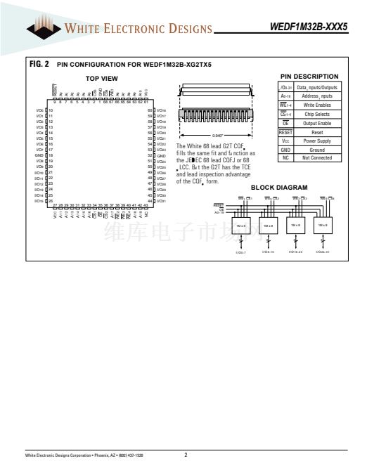
PIN CONFIGURATION FOR WEDF1M32B-XHX5
TOP VIEW
12
RESET
CS
2
GND
I/O
11
A
10
A
9
A
15
V
CC
CS
1
A
19
I/O
3
22
33
23
I/O
15
I/O
14
I/O
13
I/O
12
OE
A
17
WE
I/O
7
I/O
6
I/O
5
I/O
4
I/O
24
I/O
25
I/O
26
A
7
A
12
NC
A
13
A
8
I/O
16
I/O
17
I/O
18
44
34
V
CC
CS
4
NC
I/O
27
A
4
A
5
A
6
NC
CS
3
GND
I/O
19
55
45
I/O
31
I/O
30
I/O
29
I/O
28
A
1
A
2
A
3
I/O
23
I/O
22
I/O
21
I/O
20
1M x 8
1M x 8
1M x 8
1M x 8
RESET
WE
OE
A
0
-
19
PIN DESCRIPTION
56
I/O
0-31
A
0-19
WE
CS
1-4
OE
RESET
V
CC
GND
NC
Data Inputs/Outputs
Address Inputs
Write Enable
Chip Selects
Output Enable
Reset
Power Supply
Ground
Not Connected
BLOCK DIAGRAM
CS
1
CS
2
CS
3
CS
4
66
8
8
8
8
I/O
0-7
I/O
8-15
I/O
16-23
I/O
24-31
May 1999 Rev. 1
1
White Electronic Designs Corporation 鈥?Phoenix, AZ 鈥?(602) 437-1520


 1
1
 2
2
 3
3
 4
4
 5
5
 6
6
 7
7
 8
8
