White Electronic Designs
128Kx32 SSRAM/4Mx32 SDRAM
WED9LC6416V
EXTERNAL MEMORY SOLUTION FOR TEXAS INSTRUMENTS TMS320C6000 DSP
FEATURES
n
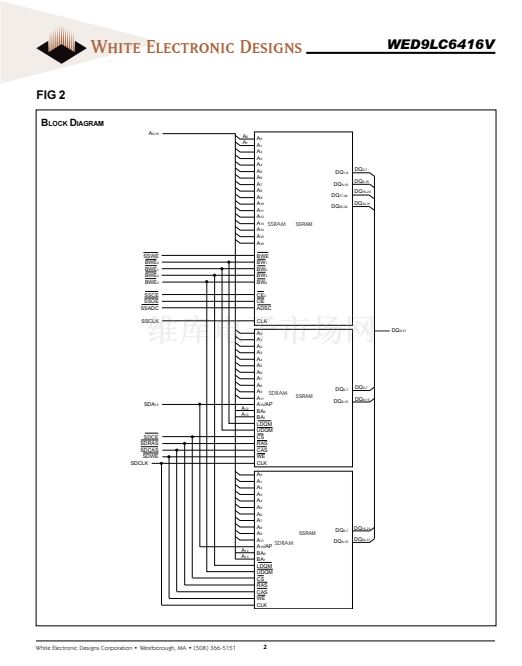
DESCRIPTION
The WED9LC6416VxxBC is a 3.3V, 128K x 32 Synchronous
Pipeline SRAM and a 4M x 32 Synchronous DRAM array
constructed with one 128K x 32 SSRAM and two 4M x 16
SDRAM die mounted on a multilayer laminate substrate. The
device is packaged in a 153 lead, 14mm by 22mm BGA.
The WED9LC6416VxxBC provides a total memory solution
for the Texas Instr uments TMS320C6201 and the
TMS320C6701 DSPs.
The Synchronous Pipeline SSRAM is available with clock
speeds of 200, 166, 150, and 133 MHz, allowing the user to
develop a fast external memory for the SSRAM interface port.
The SDRAM is available in clock speeds of 125 and 100
MHz, allowing the user to develop a fast external memory
for the SDRAM interface port.
The WED9LC6416V is available in both commercial and in-
dustrial temperature ranges.
Clock speeds:
鈥?SSRAM: 200, 166, 150, and 133 MHz
鈥?SDRAMs: 125 and 100 MHz
n
DSP Memory Solution
鈥?Texas Instruments TMS320C6201
鈥?Texas Instruments TMS320C6701
n
Packaging:
鈥?153 pin BGA, JEDEC MO-163
n
3.3V Operating supply voltage
n
Direct control interface to both the SSRAM and SDRAM
ports on the 鈥淐6x鈥?/div>
n
Common address and databus
n
65% space savings vs. monolithic solution
n
Reduced system inductance and capacitance
FIG. 1
PIN CONFIGURATION
T
OP
V
IEW
1
A
B
C
D
E
F
G
H
J
K
L
M
N
P
R
T
U
DQ
19
DQ
18
V
CCQ
DQ
17
DQ
16
V
CCQ
NC
NC
A
6
2
DQ
23
DQ
22
V
CCQ
DQ
21
DQ
20
V
CCQ
NC
NC
A
7
3
V
CC
V
CC
V
CC
V
CC
V
CC
V
CC
NC
A
8
A
9
4
V
SS
V
SS
5
V
SS
SDCE
6
V
SS
V
SS
7
V
CC
V
SS
V
CC
V
CC
V
CC
V
CC
A
2
A
1
A
0
NC
NC
V
CC
V
CC
V
CC
V
CC
V
CC
V
CC
7
8
9
A
B
C
D
E
F
G
H
J
K
L
M
N
P
R
T
U
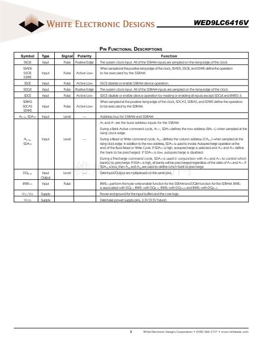
A
0-16
DQ
0-31
SSCLK
SSADC
SSWE
SSOE
SDCLK
SDRAS
SDCAS
SDWE
SDA
10
BWE
0-3
SSCE
SDCE
V
CC
V
CCQ
Vss
NC
NC/A
NX
P
IN
D
ESCRIPTION
Address Bus
Data Bus
SSRAM Clock
SSRAM Address Status Control
SSRAM Write Enable
SSRAM Output Enable
SDRAM Clock
SDRAM Row Address Strobe
SDRAM Column Address Strobe
SDRAM Write Enable
SDRAM Address 10/auto precharge
SSRAM Byte Write Enables
SDRAM SDQM 0 -3
Chip Enable SSRAM Device
Chip Enable SDRAM Device
Power Supply pins,3.3V
Data Bus Power Supply pins,
3.3V (2.5V future)
Ground
No Connect
Future Depth Expansion
DQ
24
DQ
28
DQ
25
DQ
29
V
CCQ
V
CCQ
DQ
26
DQ
30
DQ
27
DQ
31
V
CCQ
V
CCQ
A
4
A
3
A
11
A
13
A
15
A
5
A
10
A
12
A
14
A
16
SDWE SDA
10
NC
V
SS
V
SS
V
SS
V
SS
V
SS
SDCLK V
SS
V
SS
V
SS
SDRAS SDCAS V
SS
V
SS
V
SS
V
SS
V
SS
V
SS
V
SS
NC
NC
NC
NC/A
17
NC/A
18
NC/A
19
NC
V
CCQ
DQ
12
DQ
13
V
CCQ
DQ
14
DQ
15
1
NC
V
CCQ
DQ
11
DQ
10
V
CCQ
DQ
9
DQ
8
2
NC
VCC
V
CC
V
CC
V
CC
V
CC
V
CC
3
BWE
2
BWE
3
NC
BWE
0
BWE
1
NC
V
SS
V
SS
V
SS
V
SS
V
SS
V
CCQ
V
CCQ
DQ
4
DQ
5
DQ
0
DQ
1
SSCLK V
SS
V
SS
V
SS
V
CCQ
V
CCQ
DQ
6
DQ
7
8
DQ
2
DQ
3
9
SSADC SSWE NC
SSOE SSCE
4
5
NC
6
October 2001, Rev. 1
ECO # 14663
1
White Electronic Designs Corporation 鈥?(508) 366-5151 鈥?www.whiteedc.com


 1
1
 2
2
 3
3
 4
4
 5
5
 6
6
 7
7
 8
8
 9
9
 10
10
 11
11
 12
12
 13
13
 14
14
 15
15
 16
16
 17
17
 18
18
 19
19
 20
20
 21
21
 22
22
 23
23
 24
24
 25
25
 26
26
 27
27
