WED7F324XDNSN
4Mx32 / 2x4Mx32; INTEL J3 BASED, FLASH MODULE
FEATURES
聲 4Mx32 and 2x4mx32 Densities
聲 Based on Intel's Strataflash (J3) family of Flash Devices
聲 E28F320J3
聲 (32) 128Kb Erase Blocks (Symetrical)
聲 High Performance Interface Async Page Mode Reads
聲 120/25 ns Read Access Time
聲 2.7V -3.6V Vcc Operation
聲 128 bit Protection Register;
聲 64 bit Unique Device Identifier
聲 64 bit User Programmable OTP Cells
聲 Common Flash Interface (CFI)
聲 Scaleable Command Set (SCS)
聲 32 byte Write Buffer, 32M Total Erase Cycles
聲 100,000 Erase Cycles per Block
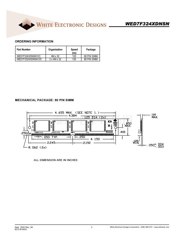
聲 Package
聲 80 pin SIMM
FIG. 1
BLOCK DIAGRAMS
WED7F324DNSN: 4Mx32 80 PIN SIMM
DESCRIPTION
The WED7F324XDNSN and WED7F2324XDNSN are organized
as one and two banks of 4Mx32 respectively. The modules are
based on Intel's E28F320J3, 4Mx8 / 2Mx16 device family. Both
modules offer access times of 120ns.
WED7F2324XDNSN: 2x4Mx32 80 PIN SIMM
Sept. 2002 Rev. 0A
ECO #15633
1
White Electronic Designs Corporation 聲 (508) 366-5151 聲 www.whiteedc.com


 1
1
 2
2
 3
3
 4
4
