White Electronic Designs
4Mx32 SDRAM
FEATURES
n
n
n
n
n
n
n
53% Space Savings vs. Monolithic Solution
Reduced System Inductance and Capacitance
Pinout and Footprint Compatible to SSRAM 119 BGA
3.3V Operating Supply Voltage
Fully Synchronous to Positive Clock Edge
Clock Frequencies of 133, 125 and 100MHz
Burst Operation
聲 Sequential or Interleave
聲 Burst Length = Programmable 1, 2, 4, 8 or Full Page
聲 Burst Read and Write
聲 Multiple Burst Read and Single Write
WED3DL324V
DESCRIPTION
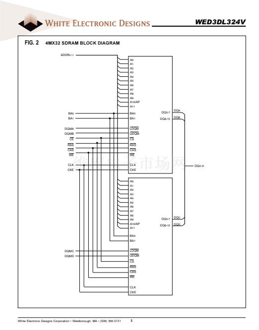
The WED3DL324V is a 4Mx32 Synchronous DRAM con-
figured as 4x1Mx32. The SDRAM BGA is constructed
with two 4Mx16 SDRAM die mounted on a multi-layer
laminate substrate and packaged in a 119 lead, 14mm
by 22mm, BGA.
The WED3DL324V is available in clock speeds of
133MHz, 125MHz and 100MHz. The range of operating
frequencies, programmable burst lengths and program-
mable latencies allow the same device to be useful for a
variety of high bandwidth, high performance memory sys-
tem applications.
The package and design provides performance enhance-
ments via a 50% reduction in capacitance vs. two mono-
lithic devices. The design includes internal ground and
power planes which reduces inductance on the ground
and power pins allowing for improved decoupling and a
reduction in system noise.
n
n
n
n
n
Data Mask Control Per Byte
Auto and Self Refresh
Automatic and Controlled Precharge Commands
Suspend Mode and Power Down Mode
119 Pin BGA, JEDEC MO-163
FIG. 1
PINOUT (TOP VIEW)
1
A
B
C
D
E
F
G
H
J
K
L
M
N
P
R
T
U
V
DDQ
NC
NC
DQ
C
DQ
C
V
DDQ
DQ
C
DQ
C
V
DDQ
DQ
D
DQ
D
V
DDQ
DQ
D
DQ
D
NC
NC
V
DDQ
1
2
NC
NC
NC
NC
DQ
C
DQ
C
DQ
C
DQ
C
V
DD
DQ
D
DQ
D
DQ
D
DQ
D
NC
A
6
NC
NC
2
3
BA
0
NC/A
12
*
BA
1
V
SS
V
SS
V
SS
DQMC
V
SS
NC
V
SS
DQMD
V
SS
V
SS
V
SS
NC
A
5
NC
3
4
NC
CAS
V
DD
NC
CE
RAS
NC
CKE
V
DD
CLK
NC
WE
A
1
A
0
V
DD
A
4
NC
4
5
A
10
A
11
A
9
V
SS
V
SS
V
SS
DQMB
V
SS
NC
V
SS
DQMA
V
SS
V
SS
V
SS
NC
A
3
NC
5
6
A
7
NC
A
8
NC
DQ
B
DQ
B
DQ
B
DQ
B
V
DD
DQ
A
DQ
A
DQ
A
DQ
A
NC
A
2
NC
NC
6
7
V
DDQ
NC
NC
DQ
B
DQ
B
V
DDQ
DQ
B
DQ
B
V
DDQ
DQ
A
DQ
A
V
DDQ
DQ
A
DQ
A
NC
NC
V
DDQ
7
A
B
C
D
E
F
G
H
J
K
L
M
N
P
R
T
U
BA0-1
DQ
CLK
CKE
DQM
RAS
CAS
CE
VDD
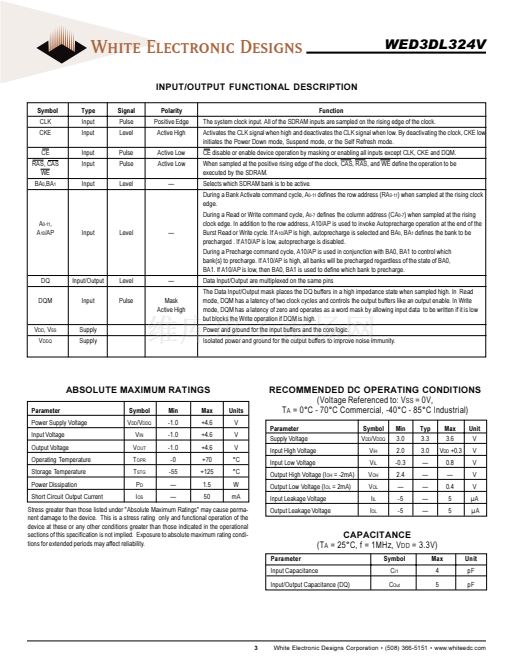
PIN DESCRIPTION
A0 聳 A11
Address Bus
Bank Select Addresses
Data Bus
Clock
Clock Enable
Data Input/Output Mask
Row Address Strobe
Column Address Strobe
Chip Enable
Power Supply pins, 3.3V
Data Bus Power Supply pins,3.3V
Ground pins
VDDQ
VSS
*NOTE:
Pin B3 is designated as NC/A
12
. This pin is used for future density upgrades as address pin A
12
.
Oct. 2001 Rev.1
ECO #15407
1
White Electronic Designs Corporation 聲 (508) 366-5151 聲 www.whiteedc.com


 1
1
 2
2
 3
3
 4
4
 5
5
 6
6
 7
7
 8
8
 9
9
 10
10
 11
11
 12
12
 13
13
 14
14
 15
15
 16
16
 17
17
 18
18
 19
19
 20
20
 21
21
 22
22
 23
23
 24
24
 25
25
 26
26
 27
27
