White Electronic Designs
WED2ZL361MSJ
1M x 36 Synchronous Pipeline Burst NBL SRAM
FEATURES
n
Fast clock speed: 250, 225, 200, 166, 150, 133MHz
n
Fast access times: 2.6, 2.8, 3.0, 3.5, 3.8, 4.2ns
n
Fast OE access times: 2.6, 2.8, 3.0, 3.5ns, 3.8ns, 4.2ns
n
Separate +2.5V 鹵 5% power supplies for core, I/O
DESCRIPTION
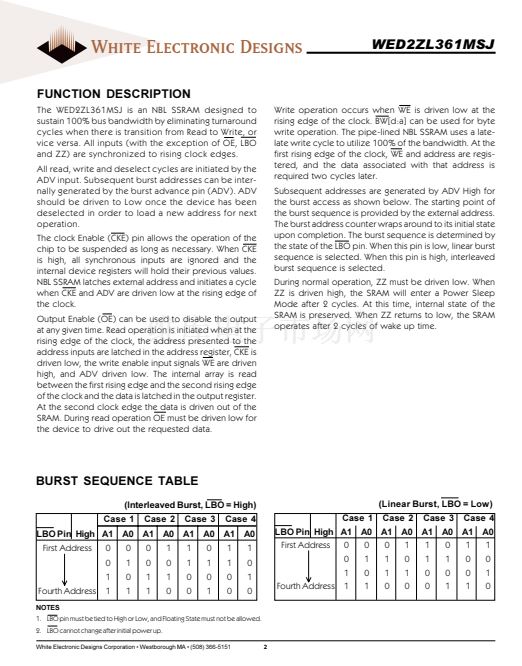
The WEDC SyncBurst - SRAM family employs high-speed,
low-power CMOS designs that are fabricated using an
advanced CMOS process. WEDC鈥檚 36Mb SyncBurst SRAMs
integrate two 1M x 18 SRAMs into a single BGA package
to provide 1M x 36 configuration. All synchronous inputs
pass through registers controlled by a positive-edge-
triggered single-clock input (CLK). The NBL or No Bus
Latency Memory utilizes all the bandwidth in any combi-
nation of operating cycles. Address, data inputs, and all
control signals except output enable and linear burst
order are synchronized to input clock. Burst order con-
trol must be tied 鈥淗igh or Low.鈥?Asynchronous inputs
include the sleep mode enable (ZZ). Output Enable
controls the outputs at any given time. Write cycles are
internally self-timed and initiated by the rising edge of
the clock input. This feature eliminates complex off-chip
write pulse generation and provides increased timing
flexibility for incoming signals.
NOTE: NBL (No Bus Latency) is equivalent to ZBT鈩?
(VDD, VDDQ)
n
Snooze Mode for reduced-standby power
n
Individual Byte Write control
n
Clock-controlled and registered addresses, data I/Os
and control signals
n
Burst control (interleaved or linear burst)
n
Packaging:
鈥?119-bump BGA package
鈥?JEDEC Pin Configuration
n
Low capacitive bus loading
FIG. 1
1
A
B
C
D
E
F
G
H
J
K
L
M
N
P
R
T
U
V
DDQ
NC
NC
DQ
c
DQ
c
V
DDQ
DQ
c
DQ
c
V
DDQ
DQ
d
DQ
d
V
DDQ
DQ
d
DQ
d
NC
NC
V
DDQ
PIN CONFIGURATION
(TOP VIEW)
2
SA
CE2
SA
DQP
c
DQ
c
DQ
c
DQ
c
DQ
c
V
DD
DQ
d
DQ
d
DQ
d
DQ
d
DQP
d
SA
NC
NC
3
SA
SA
SA
V
SS
V
SS
V
SS
BW
c
V
SS
NC
V
SS
BW
d
V
SS
V
SS
V
SS
LBO
SA
NC
4
SA
ADV
V
DD
NC
CE1
OE
SA
WE
V
DD
CLK
NC
CKE
SA1
SA0
V
DD
SA
NC
5
SA
SA
SA
V
SS
V
SS
V
SS
BW
b
V
SS
NC
V
SS
BW
a
V
SS
V
SS
V
SS
NC
SA
NC
6
SA
CE2
SA
DQP
b
DQ
b
DQ
b
DQ
b
DQ
b
V
DD
DQ
a
DQ
a
DQ
a
DQ
a
DQP
a
SA
SA
NC
7
BWc
BWd
BWa
BWb
BLOCK DIAGRAM
V
DDQ
NC
NC
DQ
b
DQ
b
V
DDQ
DQ
b
DQ
b
V
DDQ
DQ
a
DQ
a
V
DDQ
DQ
a
DQ
a
NC
ZZ
V
DDQ
Address Bus
(SA
0
鈥?SA
19
)
1M x 18
CLK
CKE
ADV
LBO
CE1
CE2
CE2
OE
WE
ZZ
CLK
CKE
ADV
LBO
CS1
CS2
CS2
OE
WE
ZZ
CLK
CKE
ADV
LBO
CS1
CS2
CS2
OE
WE
ZZ
1M x 18
DQc, DQd
DQPc, DQPd
DQa, DQb
DQPa, DQPb
DQa
鈥?/div>
DQd
DQPa
鈥?/div>
DQPd
October 2002 Rev. 1
ECO # 15465
1
White Electronic Designs Corporation 聲 (508) 366-5151 聲 www.whiteedc.com


 1
1
 2
2
 3
3
 4
4
 5
5
 6
6
 7
7
 8
8
 9
9
 10
10
 11
11
 12
12
