WED2EG472512V-D2
16MB (4x512Kx72) SYNC BURST-
PIPELINE, DUAL KEY DIMM
FEATURES
s
s
s
s
s
s
s
s
s
s
s
s
s
s
s
s
s
s
s
s
4x512Kx72 Synchronous, Synchronous Burst
Pipeline Architecture; Dual Cycle Deselect
Linear and Sequential Burst Support via MODE pin
Clock Controlled Registered Module Enable (EM)
Clock Controlled Registered Bank Enables (E
1
, E
2
, E
3
, E
4
)
Clock Controlled Byte Write Mode Enable (BWE)
Clock Controlled Byte Write Enables (BW
1
- BW
8
)
Clock Controlled Registered Address
Clock Controlled Registered Global Write (GW)
Asynchronous Output Enable (G)
Internally Self-Timed Write
Individual Bank Sleep Mode Enables (ZZ
1
, ZZ
2
, ZZ
3
, ZZ
4
)
Gold Lead Finish
3.3V
鹵
10% Operation
Frequency(s): 200, 166, 150 and 133MHz
Access Speed(s): t
KHQV
= 3.0, 3.5, 3.7 and 4.0ns
Common Data I/O
High Capacitance (30pF) Drive, at Rated Access Speed
Single Total Array Clock
Multiple V
cc
and G
nd
for Improved Noise Immunity
ADVANCED*
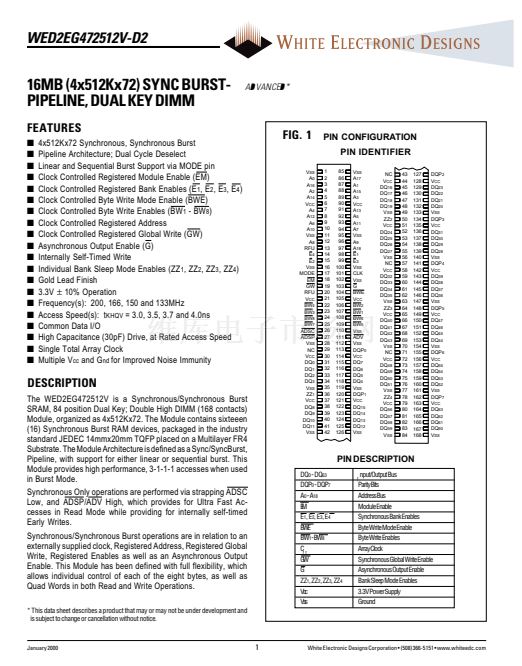
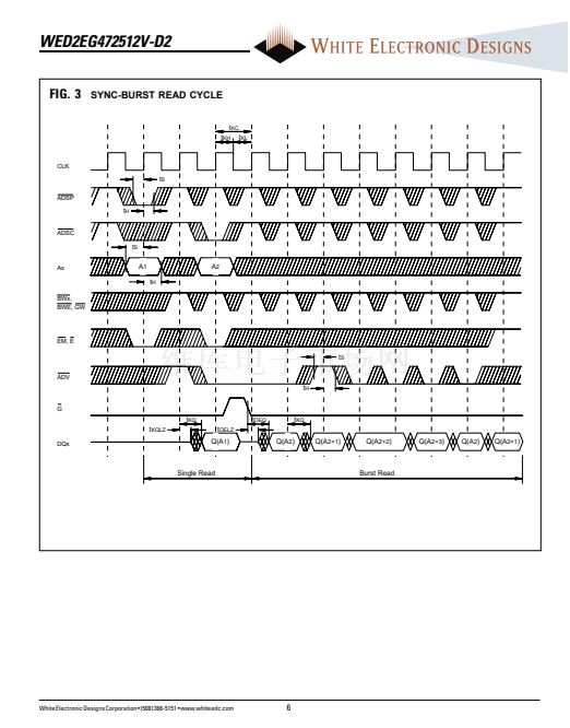
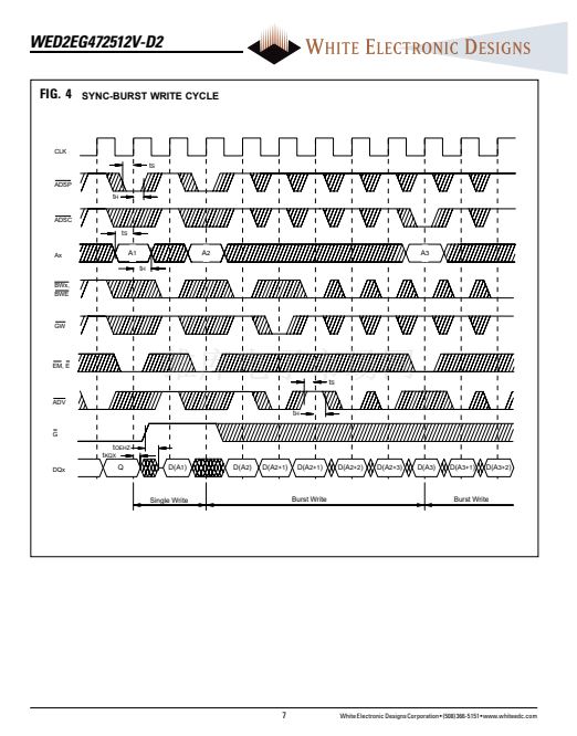
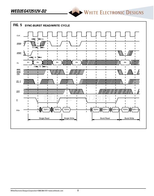
FIG. 1
V
SS
A
0
A
16
A
2
A
14
V
CC
A
4
A
12
A
6
A
10
V
SS
A
8
RFU
E
4
E
2
V
SS
MODE
EM
GW
RFU
V
CC
BW
4
BW
3
BW
8
BW
7
ADSC
ADSP
V
SS
NC
V
CC
DQ
0
DQ
1
DQ
2
DQ
3
V
SS
ZZ
1
V
CC
DQ
8
DQ
9
DQ
10
DQ
11
V
SS
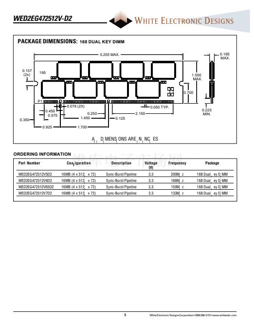
PIN CONFIGURATION
PIN IDENTIFIER
1
2
3
4
5
6
7
8
9
10
11
12
13
14
15
16
17
18
19
20
21
22
23
24
25
26
27
28
29
30
31
32
33
34
35
36
37
38
39
40
41
42
85
86
87
88
89
90
91
92
93
94
95
96
97
98
99
100
101
102
103
104
105
106
107
108
109
110
111
112
113
114
115
116
117
118
119
120
121
122
123
124
125
126
V
SS
A
17
A
1
A
15
A
3
V
CC
A
13
A
5
A
11
A
7
V
SS
A
9
A
18
E
1
E
3
V
SS
CLK
V
SS
G
BWE
V
CC
BW
2
BW
1
BW
6
BW
5
V
SS
ADV
V
SS
DQP
0
V
CC
DQ
7
DQ
6
DQ
5
DQ
4
V
SS
DQP
1
V
CC
DQ
15
DQ
14
DQ
13
DQ
12
V
SS
NC
V
CC
DQ
16
DQ
17
DQ
18
DQ
19
V
SS
ZZ
2
V
CC
DQ
24
DQ
25
DQ
26
DQ
27
V
SS
NC
V
CC
DQ
32
DQ
33
DQ
34
DQ
35
V
SS
ZZ
3
V
CC
DQ
40
DQ
41
DQ
42
DQ
43
V
SS
NC
V
CC
DQ
48
DQ
49
DQ
50
DQ
51
V
SS
ZZ
4
V
CC
DQ
56
DQ
57
DQ
58
DQ
59
V
SS
43
44
45
46
47
48
49
50
51
52
53
54
55
56
57
58
59
60
61
62
63
64
65
66
67
68
69
70
71
72
73
74
75
76
77
78
79
80
81
82
83
84
127
128
129
130
131
132
133
134
135
136
137
138
139
140
141
142
143
144
145
146
147
148
149
150
151
152
153
154
155
156
157
158
159
160
161
162
163
164
165
166
167
168
DQP
2
V
CC
DQ
23
DQ
22
DQ
21
DQ
20
V
SS
DQP
3
V
CC
DQ
31
DQ
30
DQ
29
DQ
28
V
SS
DQP
4
V
CC
DQ
39
DQ
38
DQ
37
DQ
36
V
SS
DQP
5
V
CC
DQ
47
DQ
46
DQ
45
DQ
44
V
SS
DQP
6
V
CC
DQ
55
DQ
54
DQ
53
DQ
52
V
SS
DQP
7
V
CC
DQ
63
DQ
62
DQ
61
DQ
60
V
SS
DESCRIPTION
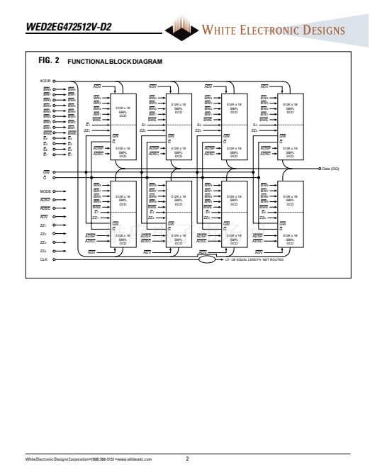
The WED2EG472512V is a Synchronous/Synchronous Burst
SRAM, 84 position Dual Key; Double High DIMM (168 contacts)
Module, organized as 4x512Kx72. The Module contains sixteeen
(16) Synchronous Burst RAM devices, packaged in the industry
standard JEDEC 14mmx20mm TQFP placed on a Multilayer FR4
Substrate. The Module Architecture is defined as a Sync/SyncBurst,
Pipeline, with support for either linear or sequential burst. This
Module provides high performance, 3-1-1-1 accesses when used
in Burst Mode.
Synchronous Only operations are performed via strapping ADSC
Low, and ADSP/ADV High, which provides for Ultra Fast Ac-
cesses in Read Mode while providing for internally self-timed
Early Writes.
Synchronous/Synchronous Burst operations are in relation to an
externally supplied clock, Registered Address, Registered Global
Write, Registered Enables as well as an Asynchronous Output
Enable. This Module has been defined with full flexibility, which
allows individual control of each of the eight bytes, as well as
Quad Words in both Read and Write Operations.
* This data sheet describes a product that may or may not be under development and
is subject to change or cancellation without notice.
PIN DESCRIPTION
DQ
0
- DQ
63
DQP
0
- DQP
7
A
0
- A
18
E
M
E
1
, E
2
, E
3
, E
4
BWE
BW
1
-BW
8
CLK
G
W
G
ZZ
1
, ZZ
2
, ZZ
3
, ZZ
4
Vcc
Vss
Input/Output Bus
ParityBits
AddressBus
Module Enable
Synchronous Bank Enables
Byte Write Mode Enable
Byte Write Enables
ArrayClock
Synchronous Global Write Enable
Asynchronous Output Enable
Bank Sleep Mode Enables
3.3VPowerSupply
Ground
January 2000
1
White Electronic Designs Corporation 鈥?(508) 366-5151 鈥?www.whiteedc.com


 1
1
 2
2
 3
3
 4
4
 5
5
 6
6
 7
7
 8
8
 9
9
