W3E32M64S-XSBX
32Mx64 DDR SDRAM
FEATURES
Advanced*
BENEFITS
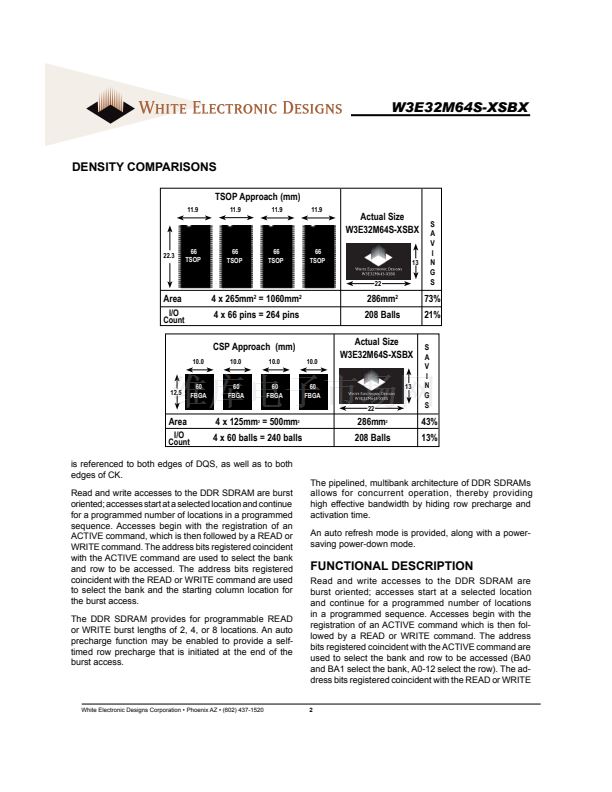
73% SPACE SAVINGS vs. TSOP
-43% Space Savings vs FPBGA
Reduced part count
21% I/O reduction vs TSOP
-13% I/O reduction vs FPBGA
Reduced trace lengths for lower parasitic
capacitance
Suitable for hi-reliability applications
Laminate interposer for optimum TCE match
Upgradeable to 64M x 64 density (contact
factory for information)
DDR SDRAM rate = 200, 250, 266
Package:
鈥?208 Plastic Ball Grid Array (PBGA),
13 x 22mm
2.5V 鹵0.2V core power supply
2.5V I/O (SSTL_2 compatible)
Differential clock inputs (CK and CK)
Commands entered on each positive CK
edge
Internal pipelined double-data-rate (DDR)
architecture; two data accesses per clock
cycle
Programmable Burst length: 2,4 or 8
Bidirectional data strobe (DQS) transmitted/
received with data, i.e., source-synchronous
data capture (one per byte)
DQS edge-aligned with data for READs;
center-aligned with data for WRITEs
DLL to align DQ and DQS transitions with
CLK
Four internal banks for concurrent operation
Data mask (DM) pins for masking write data
(one per byte)
Programmable IOL/IOH option
Auto precharge option
Auto Refresh and Self Refresh Modes
Commercial, Industrial and Military
TemperatureRanges
Organized as 32M x 64
Weight: W3E32M64S-XSBX - 2 grams typical
* Advanced data sheet describes a product that is developmental, non-quali鏗乪d
and is subject to change of cancellation without notice.
GENERAL DESCRIPTION
The 256MByte (2Gb) DDR SDRAM is a high-speed
CMOS, dynamic random-access, memory using 4 chips
containing 536,870,912 bits. Each chip is internally
configured as a quad-bank DRAM.
The 256MB DDR SDRAM uses a double data rate
ar chi tec ture to achieve high-speed operation. The
double data rate architecture is essentially a 2n-prefetch
architecture with an interface designed to transfer two
data words per clock cycle at the I/O pins. A single read
or write access for the 256MB DDR SDRAM effectively
consists of a single 2n-bit wide, one-clock-cycle data
tansfer at the internal DRAM core and two corresponding
n-bit wide, one-half-clock-cycle data transfers at the I/O
pins.
A bi-directional data strobe (DQS) is transmitted
externally, along with data, for use in data capture at the
receiver.strobe transmitted by the DDR SDRAM during
READs and by the memory contoller during WRITEs.
DQS is edge-aligned with data for READs and center-
aligned with data for WRITEs. Each chip has two data
strobes, one for the lower byte and one for the upper
byte.
The 256MB DDR SDRAM operates from a differential
clock (CK and CK); the crossing of CK going HIGH
and CK going LOW will be referred to as the positive
edge of CK. Commands (address and control signals)
are registered at every positive edge of CK. Input data
is registered on both edges of DQS, and output data
White Electronic Designs Corporation 鈥?Phoenix AZ 鈥?(602) 437-1520
January 2004 Rev. 0
1


 1
1
 2
2
 3
3
 4
4
 5
5
 6
6
 7
7
 8
8
 9
9
 10
10
 11
11
 12
12
 13
13
 14
14
 15
15
 16
16
 17
17
