W320-03
200-MHz Spread Spectrum Clock Synthesizer/Driver
with Differential CPU Outputs
Features
廬
Benefits
鈥?Compliant with Intel CK-Titan Clock Synthesizer/Driver
Supports next-generation Pentium
廬
processors using differ-
Specifications
ential clock drivers
鈥?Multiple output clocks at different frequencies
鈥?Three pairs of differential CPU outputs, up to 200 MHz
鈥?Ten synchronous PCI clocks, three free-running
鈥?Six 3V66 clocks
鈥?Two 48-MHz clocks
鈥?One reference clock at 14.318 MHz
鈥?One VCH clock
鈥?Spread Spectrum clocking (down spread)
鈥?Power-down features (PCI_STOP#, CPU_STOP#
PWR_DWN#)
鈥?OE and Test Mode support
鈥?56-pin SSOP package and 56-pin TSSOP package
Enables reduction of electromagnetic interference (EMI) and
overall system cost
Enables ACPI-compliant designs
Motherboard clock generator
鈥?Support Multiple CPUs and a chipset
鈥?Support for PCI slots and chipset
鈥?Supports AGP, DRCG reference and Hub Link
鈥?Supports USB host controller and graphic controller
鈥?Supports ISA slots and I/O chip
鈥?Three Select inputs (Mode select & IC Frequency Select)
Supports up to four CPU clock frequencies
Enables ATE and 鈥渂ed of nails鈥?testing
Widely available, standard package enables lower cost
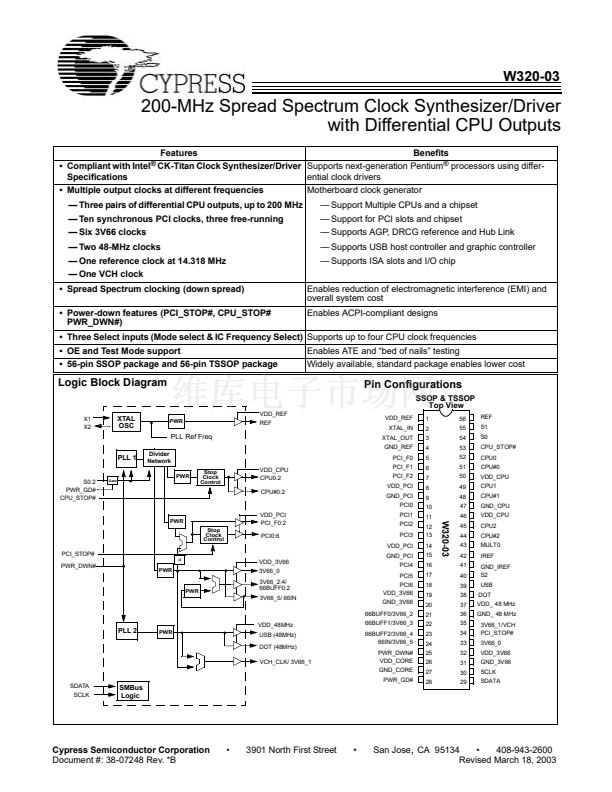
Logic Block Diagram
VDD_REF
PWR
Pin Configurations
SSOP & TSSOP
Top View
VDD_REF
XTAL_IN
XTAL_OUT
GND_REF
PCI_F0
PWR
Stop
Clock
Control
X1
X2
XTAL
OSC
REF
1
2
3
4
5
6
7
8
9
10
11
56
55
54
53
52
51
50
49
48
47
46
REF
S1
S0
CPU_STOP#
CPU0
CPU#0
VDD_CPU
CPU1
CPU#1
GND_CPU
VDD_CPU
CPU2
CPU#2
MULT0
IREF
GND_IREF
S2
USB
DOT
VDD_ 48 MHz
GND_ 48 MHz
3V66_1/VCH
PCI_STOP#
3V66_0
VDD_3V66
GND_3V66
SCLK
SDATA
PLL Ref Freq
PLL 1
S0:2
PWR_GD#
CPU_STOP#
Divider
Network
VDD_CPU
CPU0:2
CPU#0:2
PCI_F1
PCI_F2
VDD_PCI
GND_PCI
PCI0
PCI1
PCI2
PCI3
VDD_PCI
Gate
PWR
Stop
Clock
Control
VDD_PCI
PCI_F0:2
PCI0:6
W320-03
12
13
14
15
16
17
18
19
20
21
22
23
24
25
26
27
28
45
44
43
42
41
40
39
38
37
36
35
34
33
32
31
30
29
PCI_STOP#
/2
GND_PCI
VDD_3V66
3V66_0
PWR
PWR_DWN#
PWR
PCI4
PCI5
PCI6
VDD_3V66
GND_3V66
66BUFF0/3V66_2
66BUFF1/3V66_3
66BUFF2/3V66_4
66IN/3V66_5
PWR_DWN#
VDD_CORE
GND_CORE
PWR_GD#
3V66_2:4/
66BUFF0:2
3V66_5/ 66IN
PLL 2
VDD_48MHz
PWR
USB (48MHz)
DOT (48MHz)
VCH_CLK/ 3V66_1
SDATA
SCLK
SMBus
Logic
Cypress Semiconductor Corporation
Document #: 38-07248 Rev. *B
鈥?/div>
3901 North First Street
鈥?/div>
San Jose
,
CA 95134
鈥?/div>
408-943-2600
Revised March 18, 2003


 1
1
 2
2
 3
3
 4
4
 5
5
 6
6
 7
7
 8
8
 9
9
 10
10
 11
11
 12
12
 13
13
 14
14
 15
15
 16
16
 17
17
