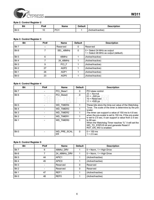
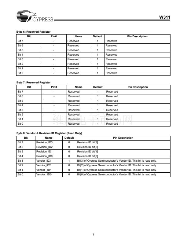
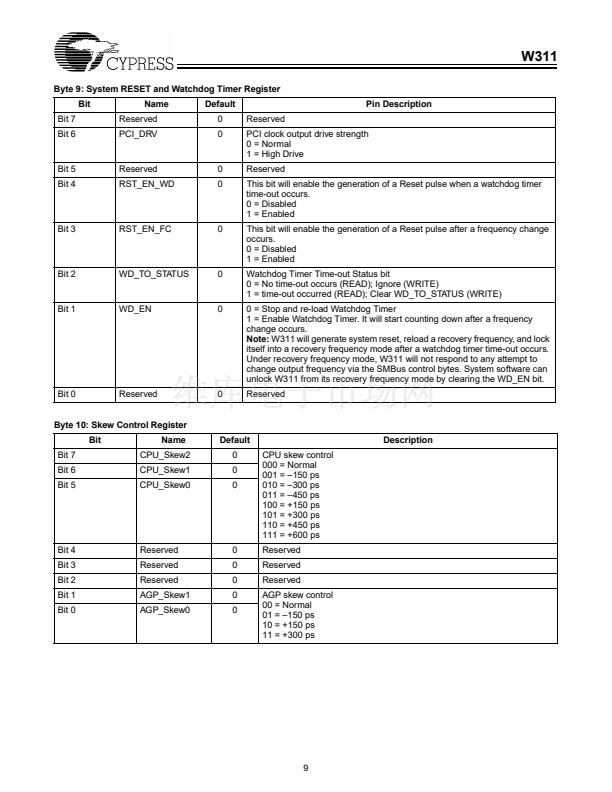
1W311
W311
FTG for VIA Pro-266 DDR Chipset
Features
鈥?Maximized EMI Suppression using Cypress鈥檚 Spread
Spectrum Technology
鈥?System frequency synthesizer for VIA Pro-2000
鈥?Programmable clock output frequency with less than
1 MHz increment
鈥?Integrated fail-safe Watchdog Timer for system
recovery
鈥?Automatically switch to HW selected or SW
programmed clock frequency when Watchdog Timer
time-out
鈥?Capable of generate system RESET after a Watchdog
Timer time-out occurs or a change in output frequency
via SMBus interface
鈥?Support SMBus byte read/write and block read/ write
operations to simplify system BIOS development
鈥?Vendor ID and Revision ID support
鈥?Programmable drive strength for CPU and PCI output
clocks
鈥?Programmable output skew between CPU, AGP and PCI
鈥?Supports Intel廬 Celeron廬 and Pentium廬 III class pro-
cessor
鈥?Three copies of CPU output
鈥?Nine copies of PCI output
鈥?One 48-MHz output for USB
鈥?One 24-MHz or 48-MHz output for SIO
鈥?Two buffered reference outputs
鈥?Three copies of APIC output
鈥?Supports frequencies up to 200 MHz
鈥?SMBus interface for programming
鈥?Power management control inputs
鈥?Available in 48-pin SSOP
Key Specifications
CPU Cycle-to-Cycle Jitter:...........................................250 ps
CPU to CPU Output Skew:..........................................175 ps
PCI Cycle to Cycle Jitter:.............................................500 ps
PCI to PCI Output Skew: .............................................500 ps
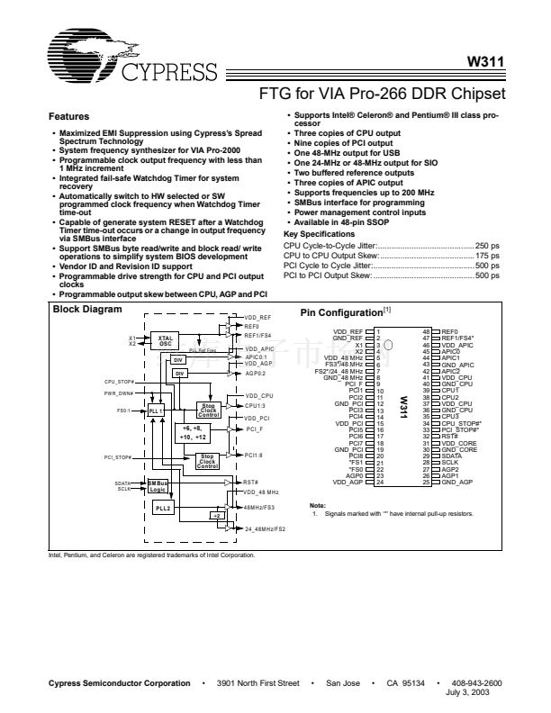
Block Diagram
V D D _R E F
R EF 0
X1
X2
XTAL
OSC
PLL Ref Freq
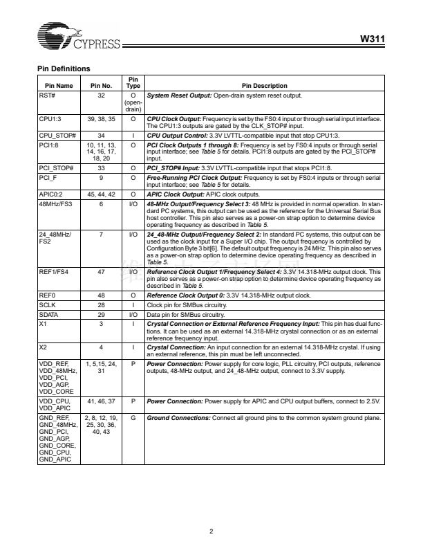
Pin Configuration
[1]
VDD_REF
GND_REF
X1
X2
VDD_48 MHz
FS3*/48 MHz
FS2*/24_48 MHz
GND_48 MHz
PCI_F
PCI1
PCI2
GND_PCI
PCI3
PCI4
VDD_PCI
PCI5
PCI6
PCI7
GND_PCI
PCI8
*FS1
*FS0
AGP0
VDD_AGP
1
2
3
4
5
6
7
8
9
10
11
12
13
14
15
16
17
18
19
20
21
22
23
24
48
47
46
45
44
43
42
41
40
39
38
37
36
35
34
33
32
31
30
29
28
27
26
25
REF0
REF1/FS4*
VDD_APIC
APIC0
APIC1
GND_APIC
APIC2
VDD_CPU
GND_CPU
CPU1
CPU2
VDD_CPU
GND_CPU
CPU3
CPU_STOP#*
PCI_STOP#*
RST#
VDD_CORE
GND_CORE
SDATA
SCLK
AGP2
AGP1
GND_AGP
R EF 1/F S 4
V D D _A P IC
A PIC 0:1
VD D _AG P
AG P 0:2
DIV
DIV
C P U _STO P #
PW R _D W N #
V D D _C P U
PLL 1
Stop
Clock
Control
C P U 1:3
V D D _P C I
P C I_F
W311
FS 0:1
梅6, 梅8,
梅10, 梅12
P C I_STO P #
Stop
Clock
Control
SM Bus
Logic
PLL2
梅2
P C I1:8
SD ATA
S C LK
RST#
V D D _48 M H z
48M H z/F S 3
Note:
1. Signals marked with 鈥?鈥?have internal pull-up resistors.
24_48M H z/F S2
Intel, Pentium, and Celeron are registered trademarks of Intel Corporation.
Cypress Semiconductor Corporation
鈥?/div>
3901 North First Street
鈥?/div>
San Jose
鈥?/div>
CA 95134
鈥?/div>
408-943-2600
July 3, 2003


 1
1
 2
2
 3
3
 4
4
 5
5
 6
6
 7
7
 8
8
 9
9
 10
10
 11
11
 12
12
 13
13
 14
14
 15
15
 16
16
 17
17
 18
18
 19
19
