PRELIMINARY
W310
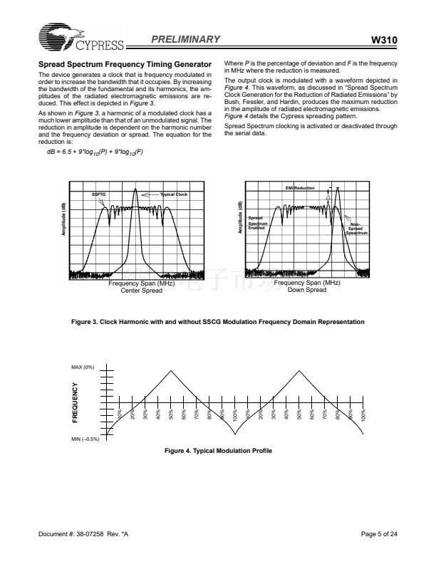
Spread Spectrum FTG for VIA K7 Chipset
Features
鈥?Single-chip system frequency synthesizer for VIA K7
chipset
鈥?Pin compatible with W210, W230 and W230-03
鈥?Programmable clock output frequency with less than
1 MHz increment
鈥?Integrated fail-safe Watchdog Timer for system recov-
ery
鈥?Automatically switch to HW selected or SW pro-
grammed clock frequency when Watchdog Timer time-
out
鈥?Capable of generate system RESET after a Watchdog
Timer time-out occurs or a change in output frequency
via SMBus interface
鈥?Support SMBus byte read/write and block read/ write
operations to simplify system BIOS development
鈥?Vendor ID and Revision ID support
鈥?Programmable drive strength for CPU, SDRAM and PCI
output clocks
鈥?Programmable output skew between CPU, PCI and
SDRAM
鈥?Maximized EMI Suppression using Cypress鈥檚 Spread
Spectrum technology
鈥?Available in 48-pin SSOP
Input Address
FS
3
1
1
1
1
1
1
1
1
0
0
0
0
0
0
FS
2
1
1
1
1
0
0
0
0
1
1
1
1
0
0
0
0
FS
1
1
1
0
0
1
1
0
0
1
1
0
0
1
1
0
0
FS
0
1
0
1
0
1
0
1
0
1
0
1
0
1
0
1
0
CPU_CS
CPUT0 (MHz)
100.0
100.0
100.0
95.0
133.3
133.3
133.3
102.0
104.0
106.0
107.0
108.0
109.0
110.0
111.0
112.0
PCI 0:5
(MHz)
33.3
33.3
33.3
31.7
33.3
33.3
33.3
34.0
34.6
35.3
35.6
36.0
36.3
36.6
37.0
37.3
Key Specifications
CPU to CPU Output Skew: ...........................................175 ps
PCI to PCI Output Skew: ..............................................500 ps
V
DD
: .........................................................................3.3V 鹵5%
SDRAMIN to SDRAM0:12 Delay: ...........................3.7 ns typ.
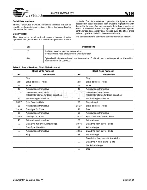
Table 1. Mode Input Table
Mode
0
1
Pin 2
CPU_STOP#
REF0
0
0
Cypress Semiconductor Corporation
Document #: 38-07258 Rev. *A
鈥?/div>
3901 North First Street
鈥?/div>
San Jose
鈥?/div>
CA 95134 鈥?408-943-2600
Revised December 19, 2002


 1
1
 2
2
 3
3
 4
4
 5
5
 6
6
 7
7
 8
8
 9
9
 10
10
 11
11
 12
12
 13
13
 14
14
 15
15
 16
16
 17
17
 18
18
 19
19
 20
20
 21
21
 22
22
 23
23
 24
24
