3
PRELIMINARY
W250-03
FTG for VIA Apollo Pro-266
Features
鈥?Maximized EMI Suppression using Cypress鈥檚 Spread
Spectrum Technology
鈥?System frequency synthesizer for VIA Apollo Pro-266
鈥?Supports Intel廬 Pentium廬 II and Pentium廬 III class pro-
cessor
鈥?Three copies of CPU output
鈥?Nine copies of PCI output
鈥?One 48-MHz output for USB
鈥?One 24-MHz or 48-MHz output for SIO
鈥?Two buffered reference outputs
鈥?Three copies of APIC output
鈥?Supports frequencies up to 200 MHz
鈥?SMBus interface for programming
鈥?Power management control inputs
鈥?Available in 48-pin SSOP
Key Specifications
CPU Cycle-to-Cycle Jitter: ................................................ 250 ps
CPU to CPU Output Skew: ............................................... 175 ps
PCI Cycle to Cycle Jitter: .................................................. 500 ps
PCI to PCI Output Skew: .................................................. 500 ps
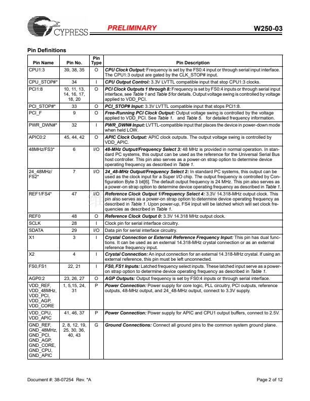
Table 1. Pin Selectable Frequency
(continued)
Input Address
FS4
0
0
0
0
0
0
0
0
0
0
0
1
1
1
1
1
1
1
1
1
PCI
(MHz)
33.3
31.7
30.0
28.3
41.5
Spread
Spectrum
OFF
OFF
OFF
OFF
OFF
1
1
1
1
1
1
1
FS3
0
0
0
1
1
1
1
1
1
1
1
0
0
0
0
0
0
0
0
1
1
1
1
1
1
1
1
FS2
1
1
1
0
0
0
0
1
1
1
1
0
0
0
0
1
1
1
1
0
0
0
0
1
1
1
1
FS1
0
1
1
0
0
1
1
0
0
1
1
0
0
1
1
0
0
1
1
0
0
1
1
0
0
1
1
FS0
1
0
1
0
1
0
1
0
1
0
1
0
1
0
1
0
1
0
1
0
1
0
1
0
1
0
1
CPU,
(MHz)
160.0
150.0
145.0
140.0
136.0
130.0
124.0
66.6
100.0
118.0
133.3
66.8
100.2
115.0
133.6
66.8
100.2
110.0
133.6
105.0
90.0
85.0
78.0
66.6
100.0
75.0
133.3
AGP
80.0
75.0
72.5
70.0
68.0
65.0
62.0
66.6
66.6
78.7
66.6
66.8
66.8
76.7
66.8
66.8
66.8
73.3
66.8
70.0
60.0
56.7
78.0
66.6
66.6
75.0
66.6
PCI
(MHz)
40.0
37.5
36.3
35.0
34.0
32.5
31.0
33.3
33.3
39.3
33.3
33.4
33.4
38.3
33.4
33.4
33.4
36.7
33.4
35.0
30.0
28.3
39.0
33.3
33.3
37.5
33.3
Spread
Spectrum
OFF
OFF
OFF
OFF
OFF
OFF
OFF
OFF
OFF
OFF
OFF
+0.25%
+0.25%
OFF
+0.25%
+0.5%
+0.5%
OFF
+0.5%
OFF
OFF
OFF
OFF
-0.5%
-0.5%
OFF
-0.5%
Table 1. Pin Selectable Frequency
Input Address
FS4
0
0
0
0
0
FS3
0
0
0
0
0
FS2
0
0
0
0
1
FS1
0
0
1
1
0
FS0
0
1
0
1
0
CPU,
(MHz)
200.0
190.0
180.0
170.0
166.0
AGP
66.6
63.3
60.0
56.7
83.0
Block Diagram
VDD_REF
REF0
X1
X2
XTAL
OSC
PLL Ref Freq
Pin Configuration
[1]
VDD_REF
GND_REF
X1
X2
VDD_48 MHz
FS3*/48 MHz
FS2*/24_48 MHz
GND_48 MHz
PCI_F
PCI1
PCI2
GND_PCI
PCI3
PCI4
VDD_PCI
PCI5
PCI6
PCI7
GND_PCI
PCI8
*FS1
*FS0
AGP0
VDD_AGP
1
2
3
4
5
6
7
8
9
10
11
12
13
14
15
16
17
18
19
20
21
22
23
24
48
47
46
45
44
43
42
41
40
39
38
37
36
35
34
33
32
31
30
29
28
27
26
25
REF0
REF1/FS4*
VDD_APIC
APIC0
APIC1
GND_APIC
APIC2
VDD_CPU
GND_CPU
CPU1
CPU2
VDD_CPU
GND_CPU
CPU3
CPU_STOP#*
PCI_STOP#*
PWR_DWN#*
VDD_CORE
GND_CORE
SDATA
SCLK
AGP2
AGP1
GND_AGP
REF1/FS4
VDD_APIC
APIC0:2
VDD_AGP
AGP0:2
VDD_CPU
DIV
DIV
CPU_STOP#
PWR_DWN#
FS0:1
W250-03
PLL 1
梅2,3,4
Stop
Clock
Control
CPU1:3
VDD_PCI
PCI_F
PCI_STOP#
Stop
Clock
Control
SMBus
Logic
PLL2
梅2
PCI1:8
SDATA
SCLK
VDD_48 MHz
48MHz/FS3
Note:
1. Signals marked with 鈥?鈥?have internal pull-up resistors.
24_48MHz/FS2
Intel and Pentium are registered trademarks of Intel Corporation.
Cypress Semiconductor Corporation
Document #: 38-07254 Rev. *A
鈥?/div>
3901 North First Street
鈥?/div>
San Jose
鈥?/div>
CA 95134 鈥?408-943-2600
Revised December 14, 2002


 1
1
 2
2
 3
3
 4
4
 5
5
 6
6
 7
7
 8
8
 9
9
 10
10
 11
11
 12
12
