W210
Spread Spectrum FTG for VIA K7 Chipset
Features
鈥?Maximized EMI Suppression using Cypress鈥檚 Spread
Spectrum technology
鈥?Single-chip system frequency synthesizer for VIA K7
chipset
鈥?One pair of differential CPU outputs for K7 Processor
鈥?One open-drain CPU output for VIA K7 chipset
鈥?Six copies of PCI output
鈥?One 48-MHz output for USB
鈥?One 24-MHz or 48-MHz output for SIO
鈥?Two buffered reference outputs
鈥?Thirteen SDRAM outputs provide support for 3 DIMMs
鈥?Supports frequencies up to 200 MHz
鈥?I
2
C鈩?interface for programming
鈥?Power management control inputs
鈥?Available in 48-pin SSOP
Table 1. Mode Input Table
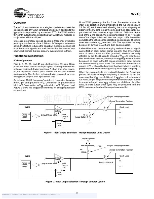
Mode
0
1
Pin 2
CPU_STOP#
REF0
Key Specifications
CPU to CPU Output Skew: ......................................... 175 ps
PCI to PCI Output Skew: ............................................ 500 ps
V
DDQ3
: .................................................................... 3.3V鹵5%
Table 2. Pin Selectable Frequency
Input Address
CPU
FS3 FS2 FS1 FS0
(MHz)
1
1
1
1
133.3
1
1
1
0
75
1
1
0
1
100.2
1
1
0
0
66.8
1
0
1
1
79
1
0
1
0
110
1
0
0
1
115
1
0
0
0
120
0
1
1
1
133.3
0
1
1
0
83.3
0
1
0
1
100.2
0
1
0
0
66.8
0
0
1
1
124
0
0
1
0
129
0
0
0
1
138
0
0
0
0
143
PCI0:5
(MHz)
33.3
37.5
33.3
33.4
39.5
36.7
38.3
30
33.3
27.7
33.3
33.4
31.0
32.3
34.5
35.8
Spread
Spectrum
鹵0.5%
鹵0.5%
鹵0.5%
鹵0.5%
OFF
OFF
OFF
OFF
OFF
OFF
OFF
OFF
OFF
OFF
OFF
OFF
Block Diagram
VDDQ3
REF0/(CPU_STOP#)
X1
X2
XTAL
OSC
PLL Ref Freq
Pin Configuration
REF1/FS0
[1]
I/O Pin
Control
PWRDWN#
CPUT_CS
Stop
Clock
Control
梅2,3,4
PLL 1
CPUT0
CPUC0
VDDQ3
PCI0/MODE
PCI1/FS1
PCI2
PCI3
PCI4
PCI5
VDDQ3
48MHz/FS2
SDATA
SCLK
I C
Logic
PLL2
梅2
2
VDDQ3
REF0/(CPU_STOP#)
GND
X1
X2
VDDQ3
PCI0/MODE
PCI1/FS1*
GND
PCI2
PCI3
PCI4
PCI5
VDDQ3
SDRAMIN
GND
SDRAM11
SDRAM10
VDDQ3
SDRAM9
SDRAM8
GND
SDATA
I
2
C
SCLK
{
1
2
3
4
5
6
7
8
9
10
11
12
13
14
15
16
17
18
19
20
21
22
23
24
48
47
46
45
44
43
42
41
40
39
38
37
36
35
34
33
32
31
30
29
28
27
26
25
REF1/FS0*
GND
CPUT_CS
GND
CPUC0
CPUT0
VDDQ3
PWRDWN#*
SDRAM12
GND
SDRAM0
SDRAM1
VDDQ3
SDRAM2
SDRAM3
GND
SDRAM4
SDRAM5
VDDQ3
SDRAM6
SDRAM7
VDDQ3
48MHz/FS2*
24_48MHz/FS3^
SDRAMIN
13
24_48MHz/FS3
VDDQ3
SDRAM0:12
Note:
1. Internal pull-up resistors should not be relied upon for setting I/O
pins HIGH. Pin function with parentheses determined by MODE pin
resistor strapping. Unlike other I/O pins, input FS3 has an internal
pull-down resistor.
W210
I
2
C is a trademark of Philips Corporation.
Cypress Semiconductor Corporation
鈥?/div>
3901 North First Street
鈥?/div>
San Jose
鈥?/div>
Powered by ICminer.com Electronic-Library Service CopyRight 2003
CA 95134 鈥?/div>
408-943-2600
April 11, 2000, rev. *C


 1
1
 2
2
 3
3
 4
4
 5
5
 6
6
 7
7
 8
8
 9
9
 10
10
 11
11
 12
12
 13
13
 14
14
