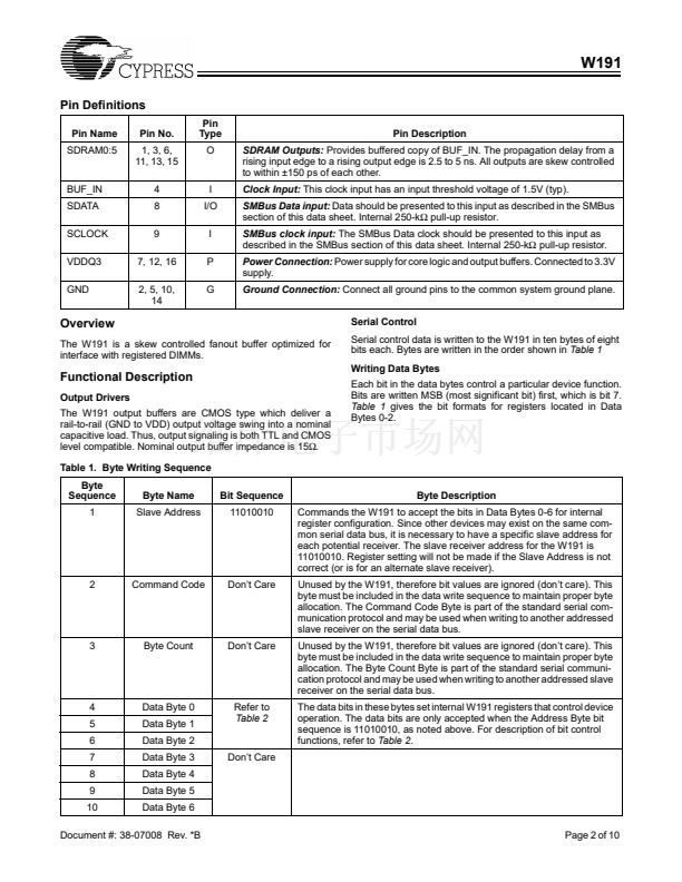
W191
Skew Controlled SDRAM Buffer
Features
鈥?Six skew controlled CMOS outputs
鈥?Output skew between any two outputs is less than
150 ps
鈥?SMBus Serial configuration interface
鈥?2.5 ns to 5 ns propagation delay
鈥?DC to 133 MHz operation (Commercial)
鈥?DC to 100 MHz operation (Industrial)
鈥?Single 3.3V supply voltage
鈥?Low power CMOS design packaged in a 16-pin SSOP
(Small Shrink Outline Package)
Key Specifications
Supply Voltages:...................................... V
DDQ3
= 3.3V 鹵5%
Operating Temperature: (Commercial) ............. 0擄C to +70擄C
Operating Temperature: (Industrial) ............. 鈥?0擄C to +85擄C
Input Threshold: .................................................. 1.5V typical
Maximum Input Voltage:...................................V
DDQ3
+ 0.5V
Input Frequency: (Commercial) ........................ 0 to 133 MHz
Input Frequency: (Industrial) ............................ 0 to 100 MHz
BUF_IN to SDRAM0:5 Propagation Delay: ...... 2.5 ns to 5 ns
Min. Output Edge Rate:............................................. 1.0V/ns
Max. Output Skew: ......................................................150 ps
Output Duty Cycle: .................................. 45/55% worst case
Output Impedance:................................................... 15鈩?typ.
Block Diagram
Pin Configuration
[1]
SDRAM0
GND
SDRAM0
SDRAM1
SDRAM2
SDATA
SCLOCK
SMBus
Device Control
1
2
3
4
5
6
7
8
16
15
14
13
12
11
10
9
VDDQ3
SDRAM5
GND
SDRAM4
VDDQ3
SDRAM3
GND
SCLK
SDRAM1
BUF_IN
GND
SDRAM2
VDDQ3
SDATA
BUF_IN
SDRAM3
SDRAM4
SDRAM5
Note:
1. Internal pull-up resistor of 250K on SDATA and SCLK.
Cypress Semiconductor Corporation
Document #: 38-07008 Rev. *B
鈥?/div>
3901 North First Street
鈥?/div>
San Jose
鈥?/div>
CA 95134 鈥?408-943-2600
Revised December 17, 2002


 1
1
 2
2
 3
3
 4
4
 5
5
 6
6
 7
7
 8
8
 9
9
 10
10
