鈥?/div>
Three interrupts are separately software-
maskable and testable
- Times-of-day alarm once/second to
once/day
- Periodic rates from 122
碌s
to 500 ms
- End of clock update cycle
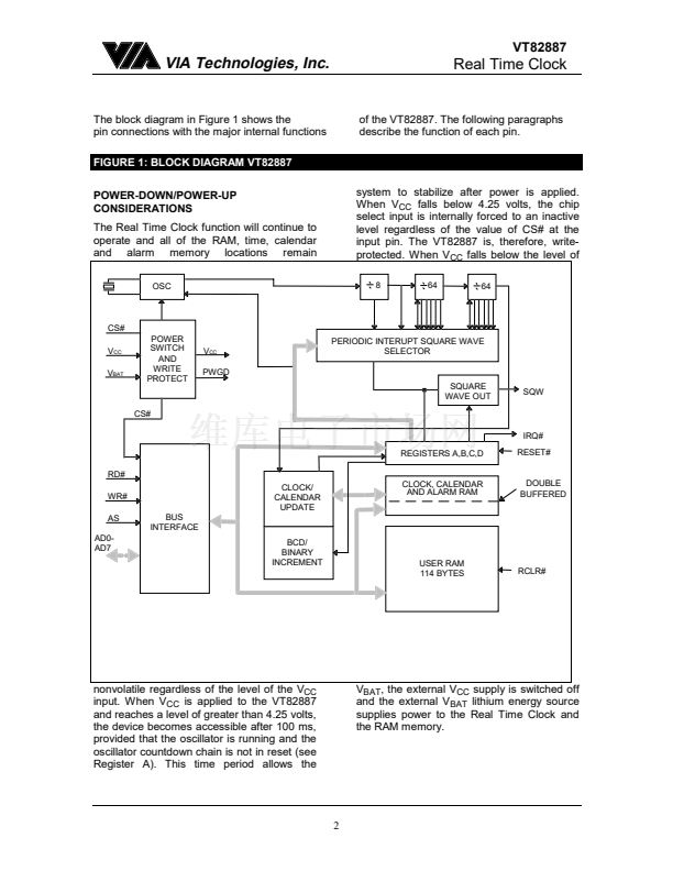
DESCRIPTION
The VT82887 Real Time Clock is designed to
be a direct replacement for the DS12887. The
VT82887 is identical in form, fit and function
to the DS12887. It has 114 bytes of general
purpose RAM. Access to this RAM space is
OPERATION
determined by the logic level presented on
AD6 during the address portion of an access
cycle. An external crystal and battery are the
only components required to maintain time-of-
day and memory status in the absence of
power. A complete description of operating
conditions, electrical characteristics, bus
timing and pin descriptions follows.
PIN ASSIGNMENT
VT82887 24 PIN DIP
GND
NC
NC
AD0
AD1
AD2
AD3
AD4
AD5
AD6
AD7
GND
1
2
3
4
5
6
7
8
9
10
11
12
24
23
22
21
20
19
18
17
16
15
14
13
V
CC
SQW
NC
RCLR#
NC
IRQ#
RESET#
RD#
NC
WR#
AS
CS#
PIN DESCRIPTION
AD0-AD7
NC
CS#
AS
WR#
RD#
RESET#
IRQ#
SQW
V
CC
GND
RCLR#
- Multiplexed Address/Data Bus
- No Connection
- Chip Select
- Address Strobe
- Write Strobe
- Read Strobe
- Reset Input
- Interrupt Request Output
- Square Wave Output
- +5 Volt Supply
- Ground
- RAM Clear
1


 1
1
 2
2
 3
3
 4
4
 5
5
 6
6
 7
7
 8
8
 9
9
 10
10
 11
11
 12
12
 13
13
 14
14
 15
15
 16
16
 17
17
