鈻?/div>
Free from secondary breakdown
Low power drive requirement
Ease of paralleling
Low C
ISS
and fast switching speeds
Excellent thermal stability
Integral SOURCE-DRAIN diode
High input impedance and high gain
Complementary N- and P-Channel devices
General Description
These enhancement-mode (normally-off) transistors utilize a
vertical DMOS structure and Supertex鈥檚 well-proven silicon-gate
manufacturing process. This combination produces devices with
the power handling capabilities of bipolar transistors and with
the high input impedance and positive temperature coef鏗乧ient
inherent in MOS devices. Characteristic of all MOS structures,
these devices are free from thermal runaway and thermally
induced secondary breakdown.
Supertex鈥檚 vertical DMOS FETs are ideally suited to a wide range
of switching and amplifying applications where high breakdown
voltage, high input impedance, low input capacitance, and fast
switching speeds are desired.
Applications
鈻?/div>
鈻?/div>
鈻?/div>
鈻?/div>
鈻?/div>
鈻?/div>
Motor controls
Converters
Ampli鏗乪rs
Switches
Power supply circuits
Drivers (relays, hammers, solenoids, lamps,
memories, displays, bipolar transistors, etc.)
Ordering Information
Device
VN3205
TO-92
VN3205N3-G
14-Lead
PDIP
VN3205P-G
TO-243AA
(SOT-89)
VN3205N8-G
Die
(1)
BV
DSS
/BV
DGS
(V)
R
DS(ON)
max
(惟)
V
GS(th)
max
(V)
VN3205ND
50
0.3
2.4
-G indicates package is RoHS compliant (鈥楪reen鈥?
Note:
(1) MIL visual screening available.
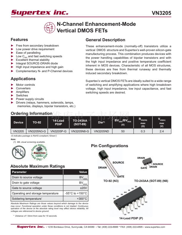
Pin Con鏗乬urations
DRAIN
SOURCE
Absolute Maximum Ratings
Parameter
Drain to source voltage
Drain to gate voltage
Gate to source voltage
Operating and storage temperature
Soldering temperature
*
Value
BV
DSS
BV
DGS
鹵20V
-55擄C to +150擄C
DRAIN
GATE
SOURCE
DRAIN
GATE
TO-92 (N3)
G3
S3
N/C
S4
G4
D4
TO-243AA (SOT-89) (N8)
D3
+300擄C
Absolute Maximum Ratings are those values beyond which damage to the device
may occur. Functional operation under these conditions is not implied. Continuous
operation of the device at the absolute rating level may affect device reliability. All
voltages are referenced to device ground.
* Distance of 1.6mm from case for 10 seconds.
D1
D2
G2
S2
N/C
S1
G1
14-Lead PDIP (P)
VN3205_07相關(guān)型號PDF文件下載
-
型號
版本
描述
廠商
下載
-
英文版
N-Channel Enhancement-Mode Vertical DMOS FETs
-
英文版
N-Channel Enhancement-Mode Vertical DMOS FETs
SUTEX [Sup...
-
英文版
N-Channel Enhancement-Mode Vertical DMOS FETs
-
英文版
N-Channel Enhancement-Mode Vertical DMOS FETs
SUTEX [Sup...
-
英文版
N-Channel Enhancement-Mode Vertical DMOS FETs
-
英文版
N-Channel Enhancement-Mode Vertical DMOS FETs
SUTEX [Sup...
-
英文版
N-Channel Enhancement-Mode Vertical DMOS FETs
-
英文版
N-Channel Enhancement-Mode Vertical DMOS FETs
SUTEX [Sup...
-
英文版
N-Channel Enhancement-Mode Vertical DMOS FETs
-
英文版
N-Channel Enhancement-Mode Vertical DMOS FETs
SUTEX [Sup...
-
英文版
暫無描述
-
英文版
Analog Buffer/Voltage Follower
ETC
-
英文版
Analog Buffer/Voltage Follower
-
英文版
Analog Buffer/Voltage Follower
ETC
-
英文版
Analog Buffer/Voltage Follower
-
英文版
Analog Buffer/Voltage Follower
ETC
-
英文版
Analog Buffer/Voltage Follower
-
英文版
Analog Buffer/Voltage Follower
ETC
-
英文版
Analog Buffer/Voltage Follower
-
英文版
Analog Buffer/Voltage Follower
ETC


 1
1
 2
2
 3
3
 4
4
 5
5
 6
6
 7
7
 8
8
