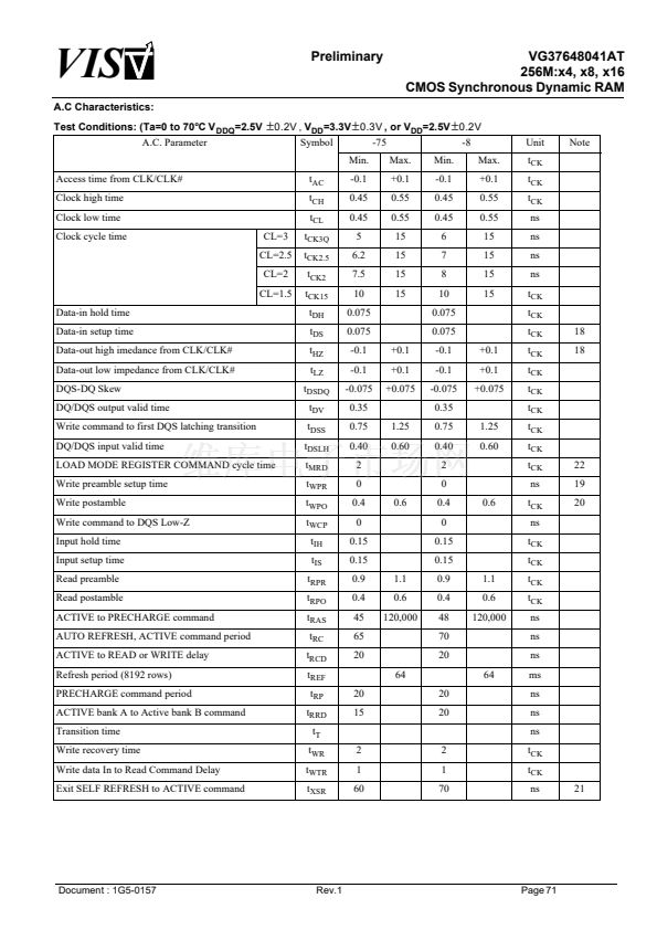
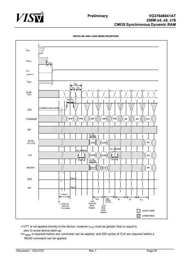
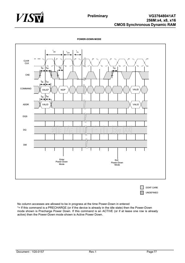
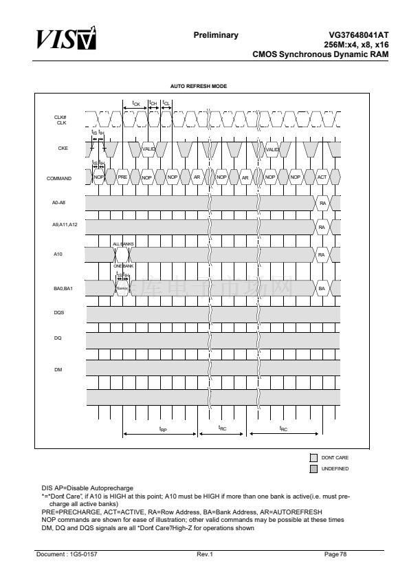
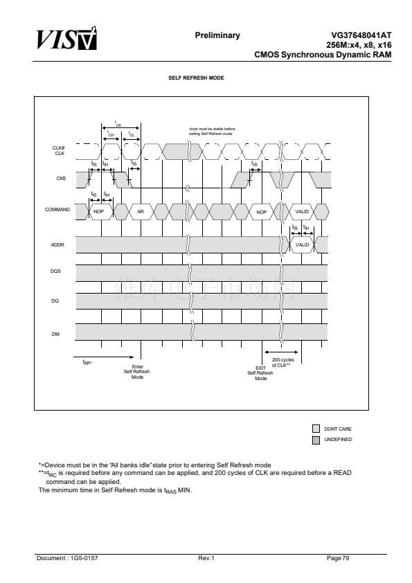
VIS
Description
Preliminary
VG37648041AT
256M:x4, x8, x16
CMOS Synchronous Dynamic RAM
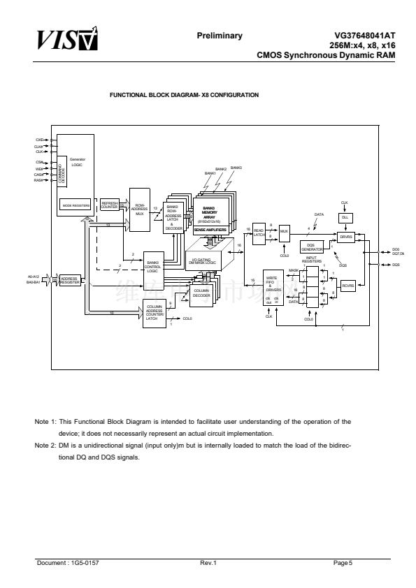
The 256Mb DDR SDRAM is a high-speed COMS, dynamic random-access memory containing
268,435,456 bits. It is internally configured as a quad-bank DRAM.
The 256Mb DDR SDRAM uses a double-data-rate architecture to achieve high-speed oper-
ation. The double data rate architecture is essentially a 2n prefetch architecture with an inter-
face designed to transfer two data words per clock cycle at the I/O pins. A single read or write
access for the 256Mb DDR SDRAM effectively consists of a single 2n-bit wide, one clock cycle
data transfer at the internal DRAM core and two corresponding n-bit wide, one-half-clock-cycle
data transfers at the I/O pins.
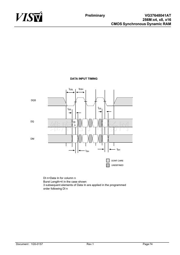
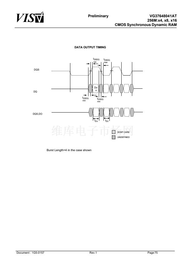
A bidirectional data strobe (DQS) is transmitted externally, along with data, for use in data
capture at the receiver. DQS is an intermittent strobe transmitted by the DDR SDRAM during
READs and by the memory controller during WRITEs. DQS is edge-aligned with data for
READs and center-aligned with data for WRITEs.
The 256Mb DDR SDRAM operates from a differential clock (CLK and CLK#; the crossing of
CLK going HIGH and CLK# going LOW will be referred to as the postive edge of CLK). Com-
mands (address and control signals) are registered at verey positive edge of CLK. Input data is
registered on both edges of DQS, and output data is referenced to both edges of DQS, as well
as to both edges of CLK.
Read and Write assesses to the DDR SDRAM are burst oriented; accesses start at a
selected location and continue for a programmed number of locations in a programmed
sequence. Accesses begin with the registration of an ACTIVE command, which is then followed
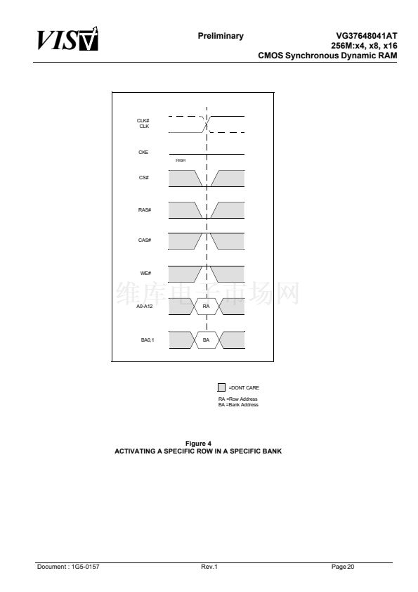
by a READ or WRITE command. The address bits registered coincident with the ACTIVE com-
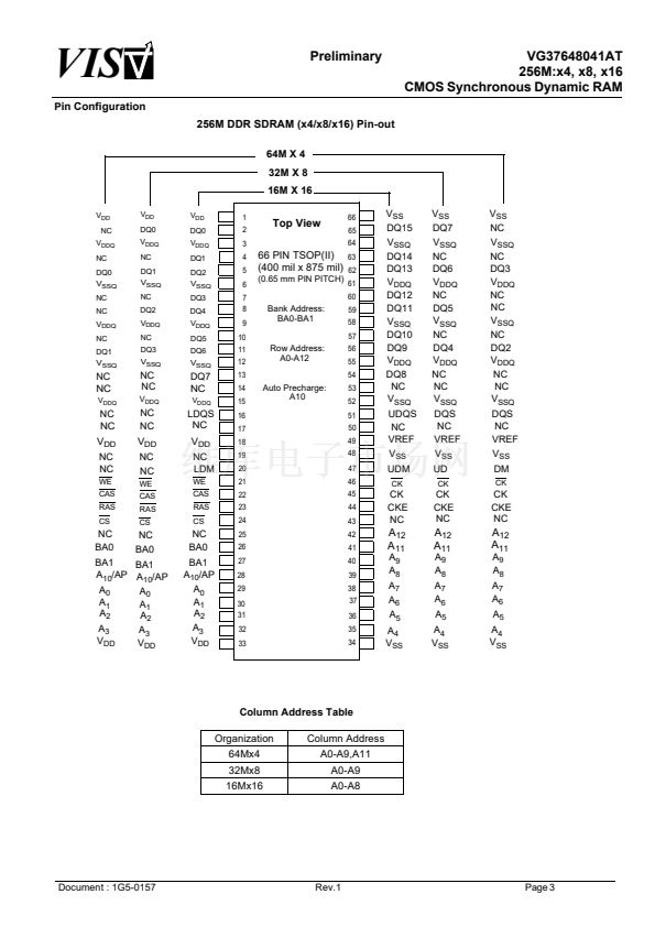
mand are used to select the bank and row to be accessed (BA0,BA1 select the bank; A0-A12
select the row). The address bits registered coincident with sthe READ or WRITE command
are used to select the starting column location for the burst access.
The DDR SDRAM provides for programmable READ or WRITE burst lengths of 2,4 or 8
locations. An AUTO PRECHARGE function may be enabled to provide a selftimed row pre-
charge that is initiated at the end of the burst access.
As with standard SDRAMs, the pipelined, multibank architecture of DDR SDRAMs allows
for concurrent operation, thereby providing high effective bandwidth by hiding row precharge
The 256Mb DDR SDRAM is designed to operate in either low-power memory systems. An
auto refresh mode is provided, along with a power-saving, power-down mode. All inputs are
compatible with the JEDEC Standard for SSTL_2. All outputs are SSTL_2, Class II compatible.
Initial devices will have a VDD supply of 3.3V (nominal). Eventually, all devices will migrate
to a VDD supply of 2.5V(nominal). During this initial period of product availability. this split will
be vendor and device specific.
This data sheet includes all features and functionality required for JEDEC DDR devices;
options not required but listed, are noted as such. Certain vendors may elect to offer a superset
of this specification by offering improved timing and/or including optional features. Users benefit
from knowing that any system design based on the required aspects of this specification are
supported by all DDR SDRAM vendors; conversely, users seeking to use any superset specifi-
cations bear the responsibility to verify support with individual vendors.
Document : 1G5-0157
Rev.1
Page 1


 1
1
 2
2
 3
3
 4
4
 5
5
 6
6
 7
7
 8
8
 9
9
 10
10
 11
11
 12
12
 13
13
 14
14
 15
15
 16
16
 17
17
 18
18
 19
19
 20
20
 21
21
 22
22
 23
23
 24
24
 25
25
 26
26
 27
27
 28
28
 29
29
 30
30
 31
31
 32
32
 33
33
 34
34
 35
35
 36
36
 37
37
 38
38
 39
39
 40
40
 41
41
 42
42
 43
43
 44
44
 45
45
 46
46
 47
47
 48
48
 49
49
 50
50
 51
51
 52
52
 53
53
 54
54
 55
55
 56
56
 57
57
 58
58
 59
59
 60
60
 61
61
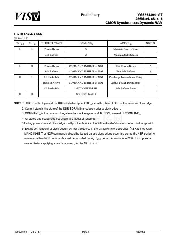 62
62
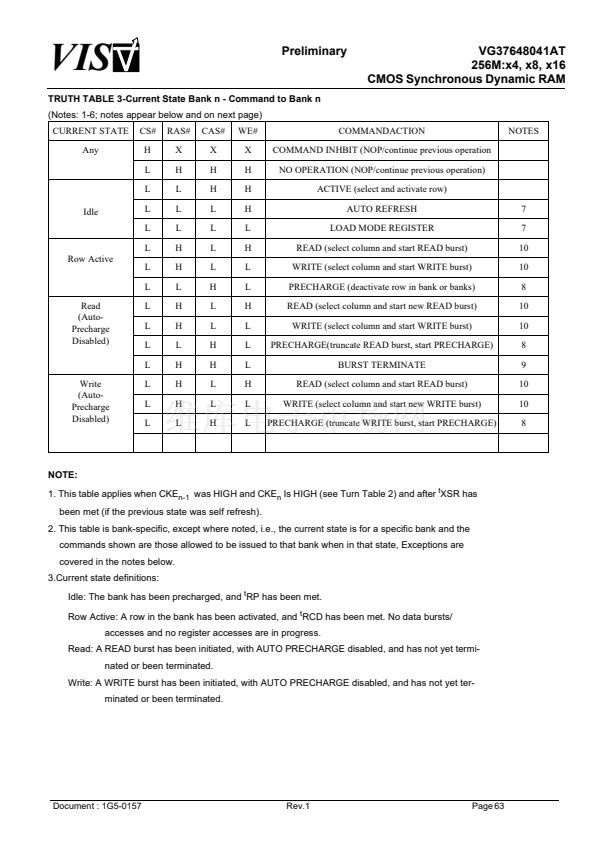 63
63
 64
64
 65
65
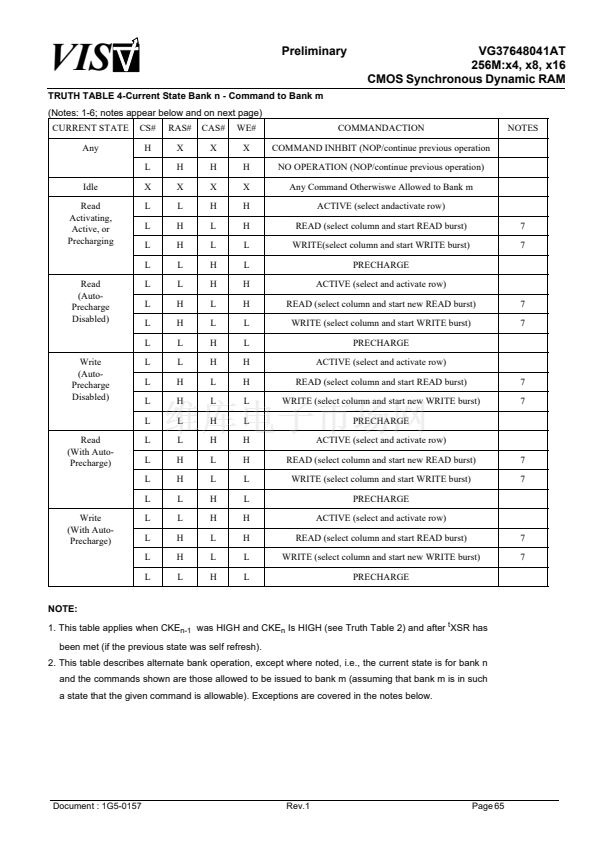
 66
66
 67
67
 68
68
 69
69
 70
70
 71
71
 72
72
 73
73
 74
74
 75
75
 76
76
 77
77
 78
78
 79
79
 80
80
 81
81
 82
82
 83
83
 84
84
 85
85
 86
86
