鈭?/div>
0.3 M A
鈭?012
M A
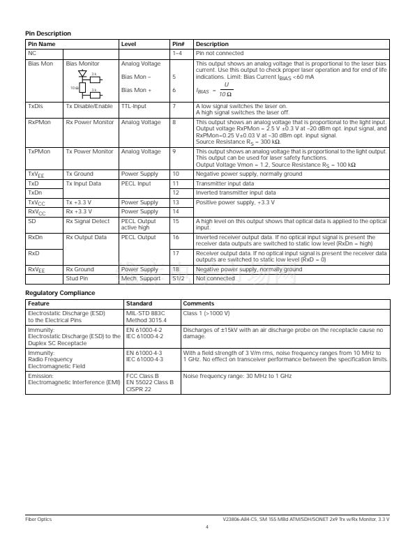
18 17 16 15 14 13 12 11 10
q
q
q
q
1
2
(25.4
鹵0.1
)
1
鹵.004
20.32
Rx
Top view
DUPLEX
SC
RECEPTACLE
q
q
q
q
q
q
q
q
q
q
q
q
q
q
3
4
5
6
7
8
9
12.7
.500
Tx
A
2.54
.100
33.02
1.3
(52 max)
2.048 max
(15.88
鹵0.5
)
.625
鹵.020
(11 max)
.433 max
Absolute Maximum Ratings
Exceeding any one of these values may destroy the device
immediately.
Package Power Dissipation
(1)
............................................ 1.5 W
Supply Voltage (V
CC
鈥揤
EE
)...................................................... 6 V
Data Input Levels.......................................................... V
CC
+0.5
Differential Data Input Voltage ............................................ 2.5 V
Operating Case Temperature.................................. 0擄 C to 70擄C
Storage Ambient Temperature ............................鈥?0擄C to 85擄C
Soldering Conditions Temp/Time
(MIL
-STD 883 C Method 2003) ............................. 250擄 C/5.5s
Note
1. For V
CC
鈥揤
EE
(min., max.). 50% duty cycle. The supply current does
not include the load drive current of the receiver output. Add max.
45 mA for the three outputs. Load is 50
鈩?/div>
to VCC鈥?2 V.
FEATURES
鈥?Compliant with ATM, SONET OC-3, SDH STM-1
鈥?Compact integrated transceiver unit with
鈥?MQW laser diode transmitter
鈥?InGaAs PIN photodiode receiver
鈥?Duplex SC receptacle
鈥?Class 1 FDA and IEC laser safety compliant
鈥?FDA Accession No. 9520890-08
鈥?Single power supply (+3.3 V)
鈥?Signal detect indicator
鈥?PECL differential inputs and outputs
鈥?Process plug included
鈥?Wave solderable and washable with process
plug inserted
鈥?Analog Rx power monitor output
鈥?Industry multisource 2x9 footprint
鈥?For distances of up to 15 km on single mode fiber
Fiber Optics
MAY 2000


 1
1
 2
2
 3
3
 4
4
 5
5
 6
6
