Standard Products
UT54LVDS031 Quad Driver
Data Sheet
June 7, 2000
FEATURES
q
q
q
q
q
q
q
q
>155.5 Mbps (77.7 MHz) switching rates
+340mV nominal differential signaling
5 V power supply
TTL compatible inputs
Ultra low power CMOS technology
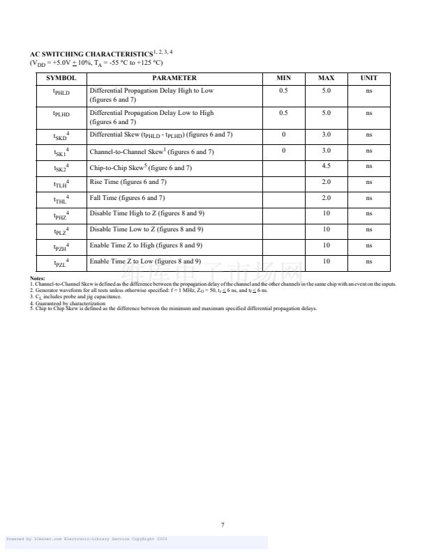
5.0ns maximum, propagation delay
3.0ns maximum, differential skew
Radiation-hardened design; total dose irradiation testing to
MIL-STD-883 Method 1019
- Total-dose: 300 krad(Si) and 1Mrad(Si)
- Latchup immune (LET > 111 MeV-cm
2
/mg)
Packaging options:
- 16-lead flatpack (dual in-line)
Standard Microcircuit Drawing 5962-95833
- QML Q and V compliant part
Compatible with IEEE 1596.3SCI LVDS
Compatible with ANSI/TIA/EIA 644-1996 LVDS Standard
INTRODUCTION
The UT54LVDS031 Quad Driver is a quad CMOS
differential line driver designed for applications requiring
ultra low power dissipation and high data rates. The device
is designed to support data rates in excess of 155.5 Mbps
(77.7 MHz) utilizing Low Voltage Differential Signaling
(LVDS) technology.
The UT54LVDS031 accepts TTL input levels and translates
them to low voltage (340mV) differential output signals. In
addition, the driver supports a three-state function that may
be used to disable the output stage, disabling the load
current, and thus dropping the device to an ultra low idle
power state.
The UT54LVDS031 and companion quad line receiver
UT54LVDS032 provide new alternatives to high power
pseudo-ECL devices for high speed point-to-point interface
applications.
q
q
q
q
D
IN1
D
OUT1+
D1
D
OUT1-
D
IN2
D
OUT2+
D2
D
OUT2-
D
OUT3+
D3
D
OUT3-
D
OUT4+
D4
D
OUT4-
D
IN3
D
IN4
EN
EN
Figure 1. UT54LVDS031 Quad Driver Block Diagram
Powered by ICminer.com Electronic-Library Service CopyRight 2003


 1
1
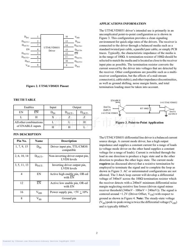 2
2
 3
3
 4
4
 5
5
 6
6
 7
7
 8
8
 9
9
 10
10
 11
11
 12
12
